Analog circuits interactive design tools & resources
Your online easy to use design companion
Recent Articles
Control
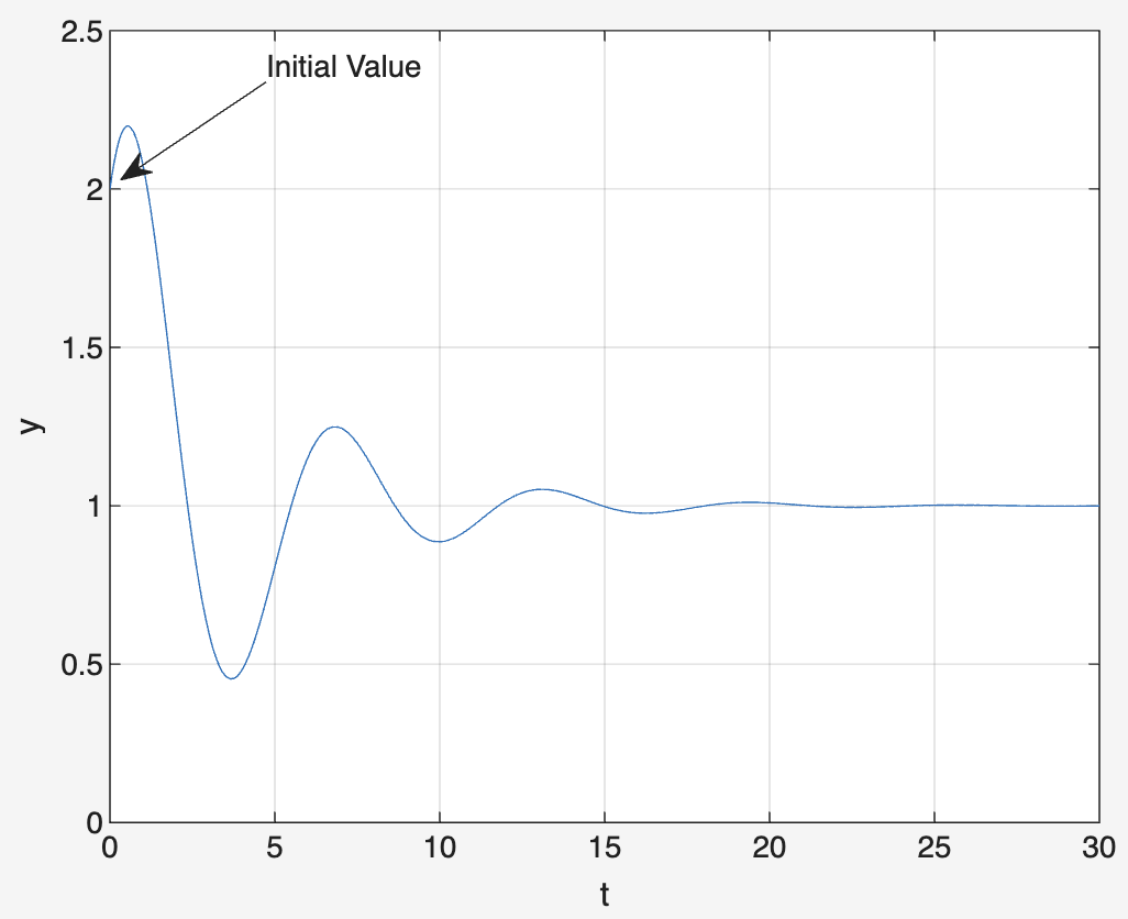
Initial Value Theorem
The initial value theorem relates the behavior of a function as time approaches zero to its Laplace transform, helping analyze system response at the start.

Data-Converters
R2R ladder digital to analog converter
An R-2R ladder DAC converts digital binary inputs into a corresponding analog voltage using a network of resistors arranged in a repeating R and 2R pattern.
Tools
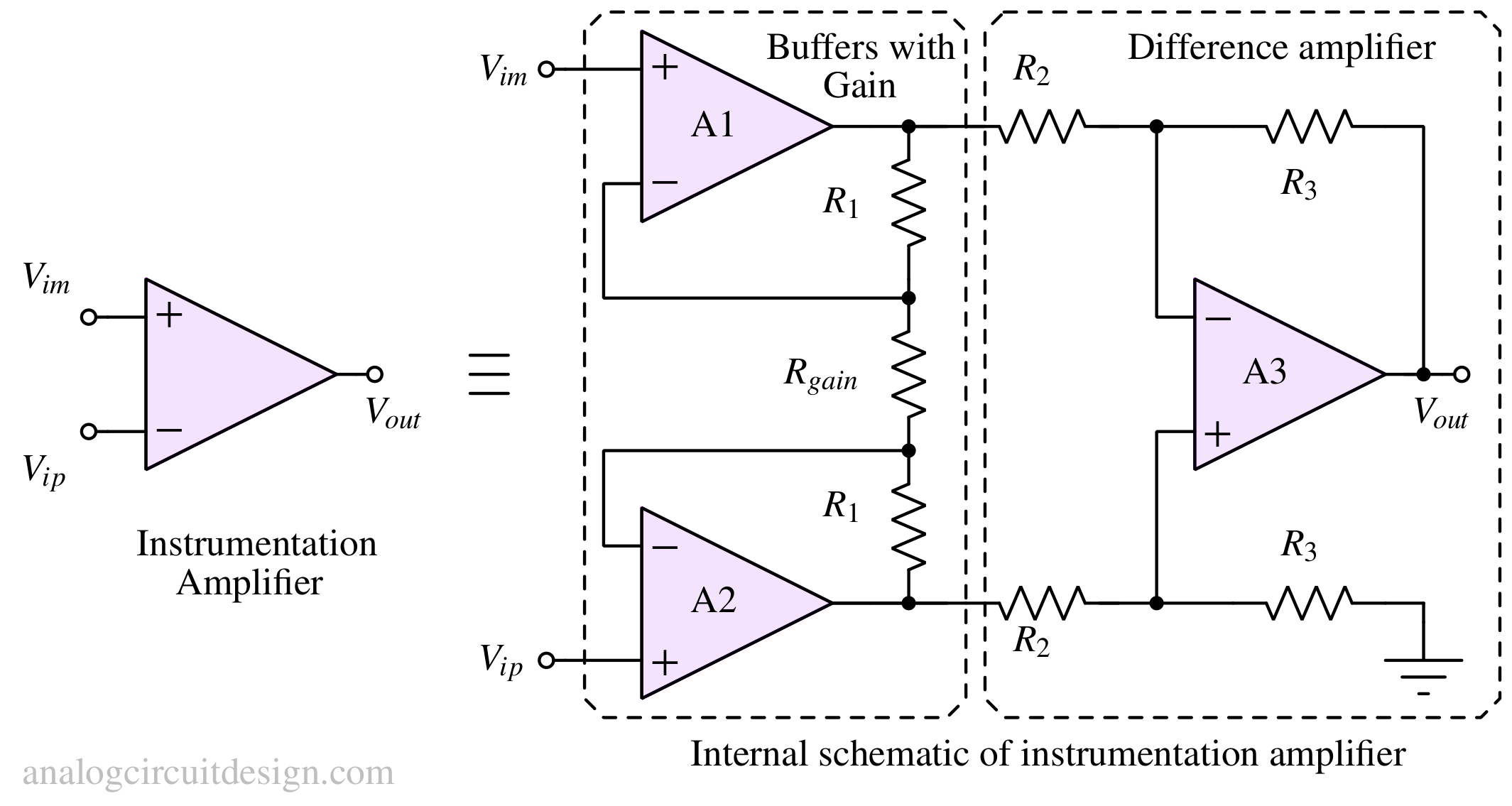
Instrumentation Amplifier Calculator
Calculate resistor values, gain of Instrumentation amplifiers