Class A Amplifier
A Class A amplifier is the simplest type of power amplifier, widely recognized for its excellent linearity and low distortion.
It has poor efficiency, as the device draws a constant current and dissipates significant power even without a signal. Despite these limitations, Class A is valued for its simplicity and excellent linearity, and role in building foundational understanding of amplifier operation. Class A amplifiers are used for low noise amplifier design due to low noise factor owing to its low component count.
Definition and Working principle
A Class A amplifier is a type of electronic amplifier in which the active device (such as a transistor or tube) conducts current during the entire cycle (360° conduction angle) of the input signal. This means it amplifies the full waveform of the input signal without turning off at any point during the cycle. The operating point (Q-point) is carefully biased in the center of the load line, which ensures that the active element never enters cutoff or saturation during normal operation, resulting in minimal distortion and high linearity.
Bias Point and Load Line Analysis

In a Class A amplifier, the device is biased at approximately the midpoint of its I–V curve (Bias point = VCC/2), allowing for a highest symmetrical voltage swing. This allows to achieve maximum signal swing and efficiency. This provides a useful first-order estimate of the DC operating point (Q-point), helping ensure maximum undistorted output in the design.
Equations :
Current through Rload:
$$I_R=\cfrac{V_{CC}-V_{CE}}{R_{load}}$$
Current through Collector of the transistor:
$$I_C=I_Se^{V_{BE}/V_t}\left(1+\cfrac{V_{CE}}{V_A}\right)$$
VA is the Early voltage associated with BJTs, VCE is collector to emitter voltage, VBE is the base to emitter voltage, Vt is kT/q which is equal to 25.6mV at 25oC.
As per KCL, IL\=IC. So both the equations, can be plotted together over VCE as shown in above figure.
Derivation of Gain formula

The small signal gain can be calculated by considering the small signal linear model of the above circuit. The small signal model is valid for other types of transistors as well (e.g., MOSFETs, JFETs) and gives a fairly close estimate. Key components are transconductance (gm) model of transistor and load (RL). The current through RL is gm x vi. The output voltage appearing is vo = gm x vi x RL. Therefore,
$$\text{Gain}=\cfrac{v_o}{v_i}=g_mR_{L}$$
This estimate is a good approximate for large signals as well as long as output voltage swing is within the linear operating range of the transistor.
Linearity and distortion
Unlike other amplifier classes (B and C) which have dead zone and cross over distortion, a Class A amplifier's transistor remains constantly conducting, therefore no dead-zone, ensuring the entire input signal is amplified.
Load configurations and Efficiency calculations
Class A amplifier can be configured in following ways depending on the applications. They have different efficiencies:
- Class A amplifier with resistive load (maximum efficiency of 25%)
- Class A amplifier with inductive load (maximum efficiency of 50%)
- Class A amplifier with transformer load (maximum efficiency of 50%)
Class A amplifier with resistive load

Efficiency : $$\eta{}=\cfrac{\text{Average signal power delivered to Load}}{\text{Average power drawn from supply}}$$ Average power delivered to load (Derivation 1): $$P_{avg,load}=\cfrac{V_{CC}^2}{8R_L}$$ Average power drawn from the power supply (Derivation 2): $$P_{avg,sup}=\cfrac{V_{CC}^2}{2R_L}$$ $$\eta{}=\cfrac{V_{CC}^2/8R_L}{V_{CC}^2/2R_L}=25%$$
Class A amplifier with inductive loading

Average power delivered to load RL (Derivation 3): $$P_{avg,load}=\cfrac{1}{2}I_L^2R_L=\cfrac{V_{CC}^2}{2R_L}$$ Average power drawn from the power supply (Derivation 4): $$P_{avg,load}=V_{CC}I_L=\cfrac{V_{CC}^2}{R_L}$$ $$\eta{}=\cfrac{V_{CC}^2/2R_L}{V_{CC}^2/R_L}=50%$$ An inductively-loaded circuit enables a lower supply voltage for a given voltage swing.
Class A amplifier with Transformer loading

Transformer loading a class A amplifier does not improve its efficiency. However it helps doing load transformation.
For example : 30W to a 4 Ohm speaker on a 5V supply?
Solution : Required voltage swing across the speaker to deliver 30W of power to the speaker :
$$\cfrac{V_{speaker}^2}{2R_L} = 30,\text{W}$$
RL = 4 Ohms. Therefore, Vspeaker is 15.5V. The maximum voltage swing which can be achieved at the primary windings of the transformer is 5V. So, the required transformer ratio is :
$$\cfrac{N}{1}=\cfrac{15.5}{5}=3.1$$
To deliver 30W of power to speaker, the power taken from the supply is 60W. Dissipating 30W (50%) of the energy as heat.
DC and AC coupling of a class A amplifier
DC coupled class A amplifier

This amplifier amplifies signal from DC to high cut-off frequency (fH). This does not have a lower cutoff frequency. Not ideal for audio applications as the input signal can disturb DC biasing condition of the class A amplifier. fH is decided by the load impedance. If there are no intentional capacitors added, the fH is limited by parasitic capacitance. The flat-band gain is gmZload.
AC coupled class A amplifier

An AC coupling capacitor is added at the input to reject frequency lesser than fL. Now this class A amplifier is effectively a bandpass filter. The lower cutoff frequency (fL) is decided by C1 and R1 || R2. The upper cutoff frequency is decided by load network. If C1 is added, CE should be added to increase the gain at passband frequency. The flat-band voltage gain becomes gmZload.
How CE is increasing the gain ? RE is a degeneration resistor which is meant to reduce the temperature dependence of BJT. However, it also lowers the DC gain. Our requirement is gain for AC signals, so during AC signals (f > 1/2*π*RECE), the CE shorts RE and increase the effective transconductance of the BJT.
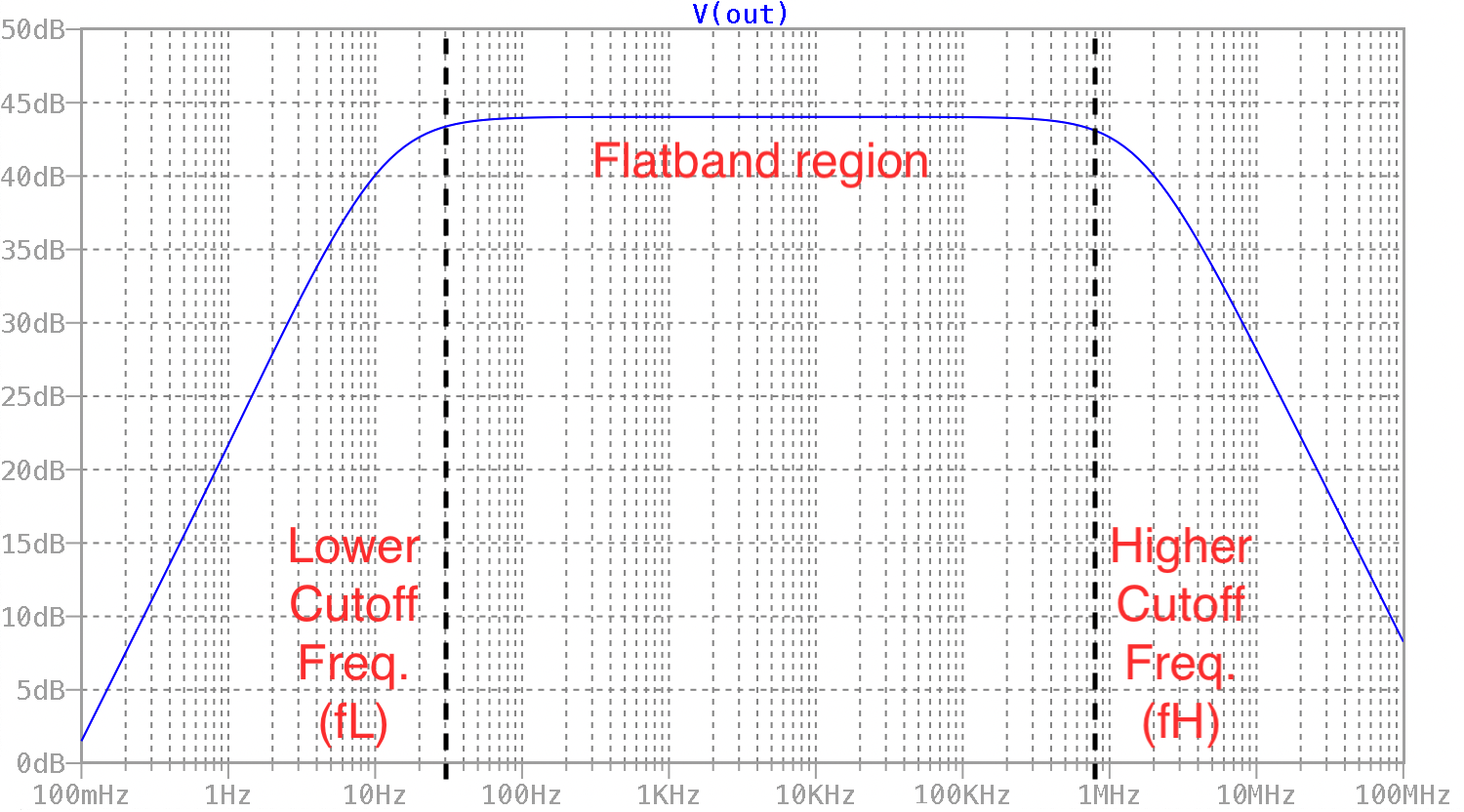
Frequency response of AC coupled class A amplifier
Class A amplifier circuit design and block diagram
Using BJTs
BJT Common Emitter (CE) configuration can be classified as a Class A amplifier. CE stage made using NPN can sink a lot of current but source very limited amount of current.

BJT Common Collector (CC) configuration also act as a class A amplifier (more specifically a power amplifier). Another important characteristic of common collector Class A amplifier (NPN type) is that they can give a lot of current while sourcing and very limited current while sinking.

Using MOSFET or JFET
MOSFET / JFET Common Source (CS) configuration can be classified as a Class A amplifier. CS stage made using NMOS can sink a lot of current but source very limited amount of current. There is no need of Darlington configuration because the gate-current is zero in MOSFET / JFET.

NMOS Common Drain (CD) configuration also act as a class A amplifier (more specifically a power amplifier). Another important characteristic of Common Drain Class A amplifier (NMOS based) is that they can give a lot of current while sourcing and very limited current while sinking.

Derivation 1
$$P_{avg,load}=\cfrac{\int_0^TP\cdot{}dt}{T}$$ $$=\cfrac{\int_0^T\cfrac{V_{out}^2}{R_L}\cdot{}dt}{T}$$ $$=\cfrac{\int_0^T\cfrac{V_p^2\sin{}^2(\omega{}_ot)}{R_L}dt}{T}$$ $$=\cfrac{\cfrac{V_p^2}{2R_L}\int_0^T2\sin{}^2(\omega{}_ot)dt}{T}$$ $$=\cfrac{\cfrac{V_p^2}{2R_L}\int_0^T(1-cos{}(2\omega{}_ot))dt}{T}$$ $$=\cfrac{\cfrac{V_p^2}{2R_L}T-\left[\cfrac{\sin{}(2\omega{}_ot)}{2\omega{}_o}\right]_0^T}{T}$$ $$=\cfrac{V_p^2}{2R_L}$$ $$V_p=\cfrac{V_{CC}}{2}$$ $$\implies{}P_{avg,load}=\cfrac{V_{CC}^2}{8R_L}$$
Derivation 2
$$P_{avg,sup}=\cfrac{\int_0^TP\cdot{}dt}{T}$$ $$=\cfrac{\int_0^TV_{CC}I_{R}dt}{T}$$ $$=\cfrac{\int_0^TV_{CC}\cfrac{V_{CC}-V_{out}}{R_L}dt}{T}$$ $$V_{out}=\cfrac{V_{CC}}{2}+V_p\sin{}(\omega{}_ot)$$ $$V_p=\cfrac{V_{CC}}{2}$$ $$P_{avg,sup}=\cfrac{V_{CC}^2}{2R}$$
Derivation 3
$$P_{avg,sup}=\cfrac{\int_0^TP\cdot{}dt}{T}=\cfrac{\int_0^Ti_R^2R_Ldt}{T}$$ $$=\cfrac{\int_0^TI_p^2R_Ldt}{T}$$ $$=\cfrac{1}{2}I_p^2R_L$$ Let's understand the DC condition of the circuit. The Inductor is behaving as a short, so the left terminal of the capacitor is at VCC. The resistor has pulled down the capacitor's right terminal to ground. So, the capacitor is now charged to VCC. When the transistor has pulled down collector node down to zero, left terminal of the resistor is at -VCC. So, the current through the resistor is -VCC/RL. When the transistor's input voltage is low, transistor is near to cut-off region. Entire inductor current flows through the capacitor and resistor. The magnitude of the inductor current (IL) should be > VCC/RL to support symmetric swing across the load. The collector voltage reaches 2VCC. Therefore, the power delivered to the load is: $$P_{avg,load}=\cfrac{1}{2}I_p^2R_L=\cfrac{V_{CC}^2}{2R_L}$$
Derivation 4
$$P_{avg,sup}=\cfrac{\int_0^TP\cdot{}dt}{T}$$ The current drawn from the supply is always IL. So, the power drawn is VCCIL = VCC2/RL