Common Base Amplifier
The common-base (CB) amplifier is a single transistor BJT amplifier with base grounded. Input terminal is emitter and output terminal is collector. It behaves as a current controlled current source. Since it has a low input resistance, the CB amplifier is the most appropriate type for certain applications where input is a current source. Current sources have very high output impedances.
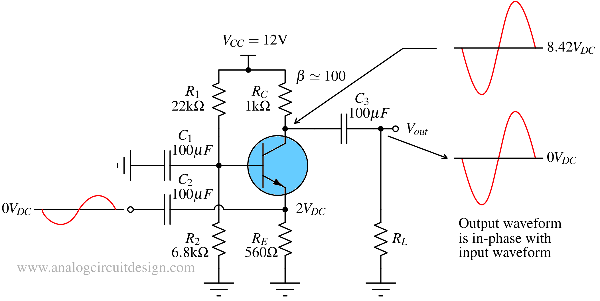
R1 & R2 are there to set the DC bias of the transistor primarily. The value of R1 and R2 should be chosen such that the base current IB does not create significant voltage drop across R1||R2, otherwise VBE junction won't turn on.
RE sets the emitter and collector current of the amplifier. It also helps prevent excess current flowing through the VBE junction and prevents thermal run-away. The collector current establishes the gm (transconductance) of the BJT.
RC, RL and gm set the gain of the amplifier.
RL is the load resistor which emulates the input impedance of following stage. It is not strictly necessary for the operation of the amplifier. RL along with C3 ensures that the output will be at 0V when input is zero.
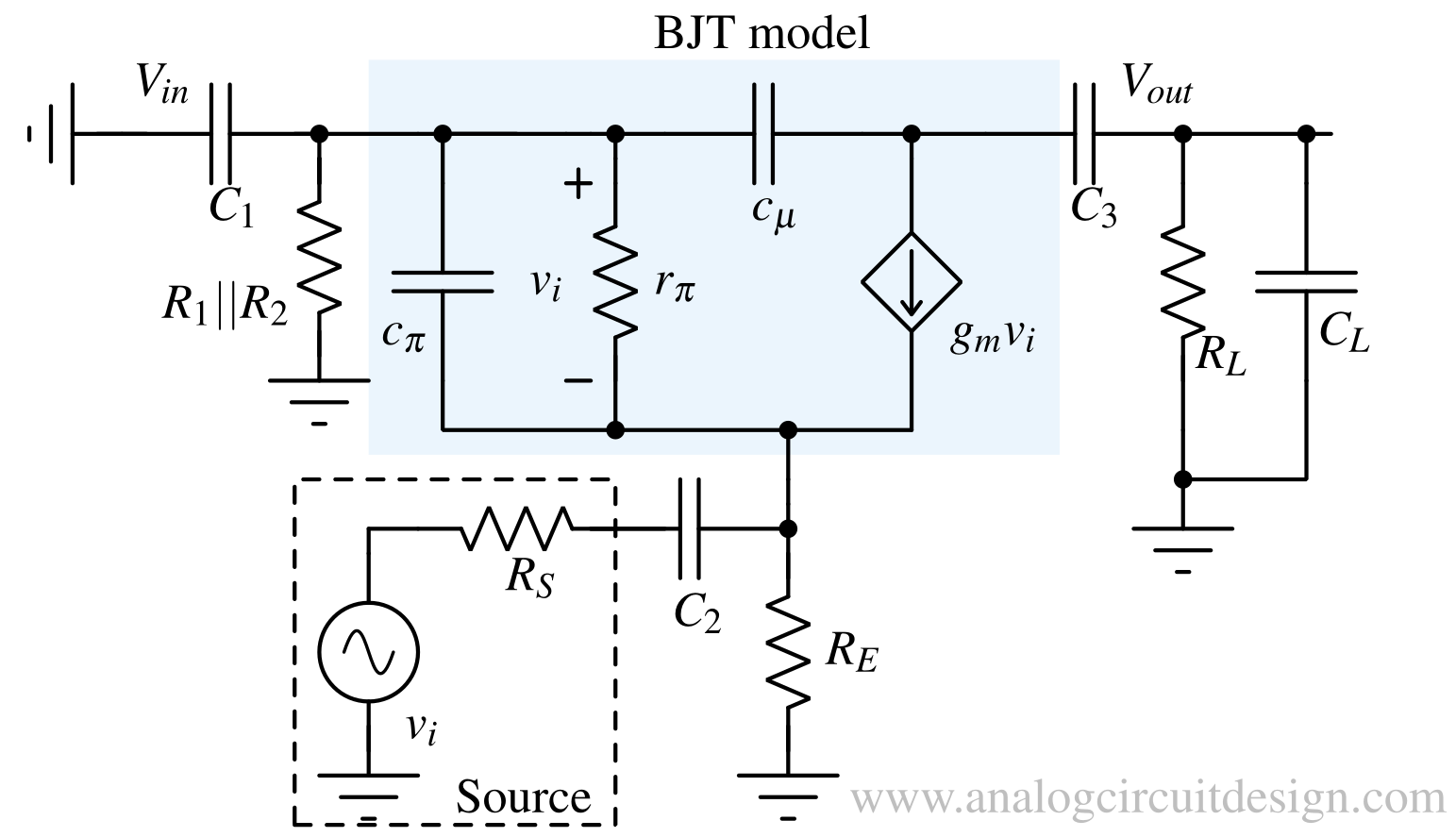
C1 is the AC bypass capacitor. It bypasses R1 and R2 at high frequency which lowers the base impedance at high frequency.
C2 is the input AC coupling capacitor. It allows the input signal and the base voltage of the transistor to have different DC voltage.
C3 is the output AC coupling capacitor. It allows output load voltage to be set independently of collector voltage.
DC analysis
To get the DC operating points, the capacitors are replaced with open circuits in the above schematic.

The goal is to obtain the VCE voltage of the amplifier which gives us the maximum possible output voltage. Also, we need to find the value of collector current which will be used to find the transconductance (gm). To simplify the circuit, lets find the Thevenin equivalent circuit :
$$R_{TH}=\cfrac{R_1R_2}{R_1+R_2}=\cfrac{(6.8\,\text{k}\Omega{})\,(22\,\text{k}\Omega{})}{6.8\,\text{k}\Omega{}+22\,\text{k}\Omega{}}=5.19\,\text{k}\Omega{}$$
$$V_{TH}=\left(\cfrac{R_2}{R_1+R_2}\right)V_{CC}=\left(\cfrac{6.8\,\text{k}\Omega{}}{6.8\,\text{k}\Omega{}+22\,\text{k}\Omega{}}\right)12\,\text{V}=2.83\,\text{V}$$
KVL,
$$V_{TH}-I_BR_{TH}-V_{BE}-(I_C+I_B)R_E=0$$
Also,
$$I_C=\beta{}I_B$$
$$\implies{}V_{TH}-\cfrac{I_C}{\beta{}}R_{TH}-V_{BE}-I_C(1+\cfrac{1}{\beta{}})R_E=0$$
$$\implies{}I_C=\cfrac{V_{TH}-V_{BE}}{(R_{TH}+R_E)/\beta{}+R_E}\simeq{}3.58\,\text{mA}$$
Emitter Voltage,
$$V_E=I_ER_E=(3.58\,\text{mA})(560 \Omega{})=2.00\,\text{V}$$
Base voltage,
$$V_B=V_E+0.7\,\text{V}=2.70\,\text{V}$$
Collector voltage,
$$V_C=V_{CC}-I_CR_C=12\,\text{V}-(3.58\,\text{mA})(1\,\text{k}\Omega{})=8.42\,\text{V}$$
Collector-Emitter voltage,
$$V_{CE}=V_C-V_E=8.42-2=6.42\,\text{V}$$
The Collector-Emitter voltage should not be less than 200mV. Otherwise, the BJT will go into saturation and gain will be zero.
Small signal analysis
BJT like any other real transistor is a non-linear device. To simplify the analysis, a BJT is converted into linear model called small-signal model as shown below. This model is not valid for DC however it is valid for flatband region and widely used in designing circuits. Beyond flatband region, we need to capture some more capacitors in the model which is shown in this section : Frequency response and bandwidth.
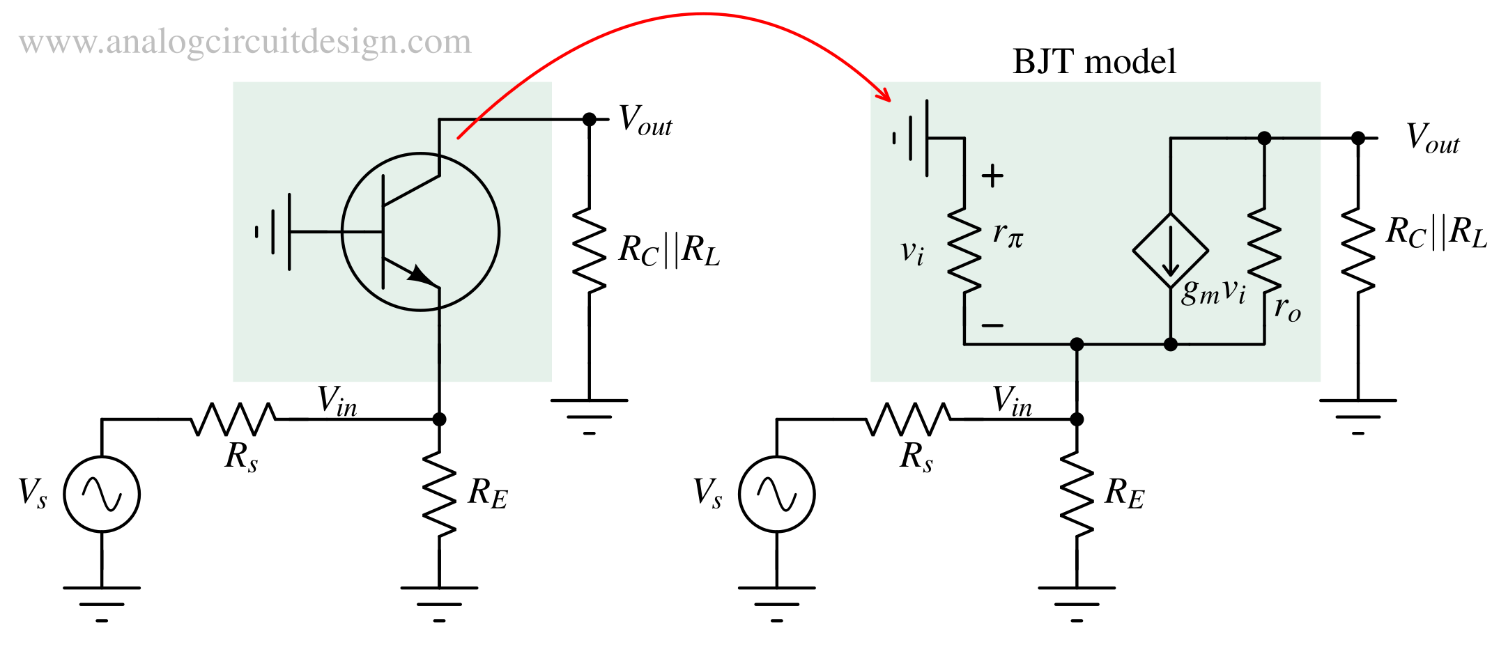
The model shown above is very useful to quickly calculate the gain of the circuit. To determine bandwidth of the circuit, we need small signal high-frequency model as it captures the internal capacitors of the BJT.
Transconductance
The transistor can be replaced by a transconductor and an input resistor. This model is applicable in any BJT configuration (Common-base, Common-collector, Common-emitter).
The transconductance gm is given by :
$$g_m=\cfrac{I_C}{V_T}$$
$$g_m=\cfrac{3.58\,\text{mA}}{25.6\,\text{mV}}=139\,\text{mS}$$
Input resistance
To compute the input impedance, we need to extract the small signal model from the above figure as follows:
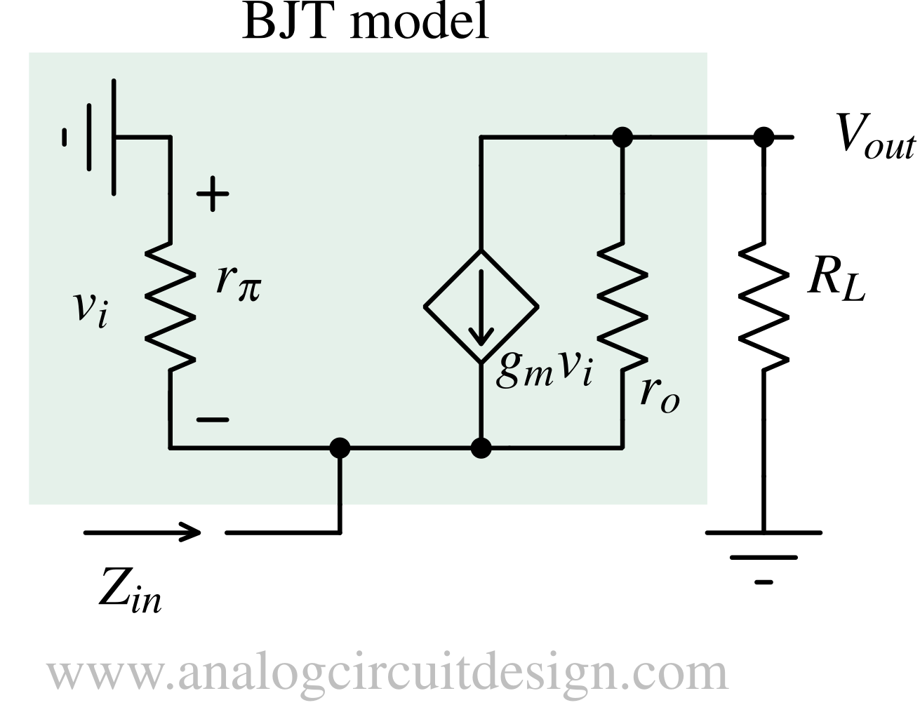
The input impedance (Zin) :
$$Z_{in}=\cfrac{1}{\cfrac{1}{r_{\pi}}+\left(\cfrac{1+g_mr_o}{R_L+r_o}\right)}$$
Case 1 : If RL is infinite (RL >> ro), the input impedance is :
$$Z_{in}=r_{\pi{}}$$
Case 2 : If RL is zero (short-circuit or RL << ro), the input impedance is :
$$Z_{in}=r_{\pi}||r_o||\cfrac{1}{g_m}\simeq{}\cfrac{1}{g_m}$$
Usually, to find the input impedance, we short the RL, therefore Case 2 is most common.
In this case,
$$Z_{in}\simeq{}\cfrac{1}{g_m}\simeq{}7.1\,\Omega{}$$
The input impedance of common-base amplifier is low in comparison to input impedance of common-emitter and common-collector amplifier.
Output resistance
The small signal output resistance is :
$$r_o=\cfrac{V_A}{I_C}$$
Where VA is the Early-voltage and IC is the collector current. If VA = 400V and IC = 3.58mA,
$$r_o=\cfrac{400\,\text{V}}{3.58\,\text{mA}}=111\,\text{k}\Omega{}$$
Voltage gain
Refering to figure shown in AC analysis, the output voltage (Vout) is :
$$V_{out}=+g_mv_iR_C$$
The output impedance (ro) has been assumed to very high (ro >> RC). The voltage gain of the BJT in Common Base configuration is :
$$A_v=\cfrac{V_{out}}{v_i}=+g_mR_C$$
Notice that there is no negative sign in the gain expression. This means that the output waveform is in phase with the input waveform. However, due to presence of source resistance Rs & RL, the voltage gain drops. To calculate, lets find the effective input voltage. The input voltage (Vin or vi) is :
$$v_{i}=\cfrac{(1/g_m)||R_E}{(1/g_m)||R_E+R_S}V_s$$
Now the effective voltage gain can be denoted by :
$$\cfrac{V_{out}}{V_{i}}=-g_mR_C\cfrac{(1/g_m)||R_E}{(1/g_m)||R_E+R_S}$$
It can be observed that the voltage gain is dependent on source resistance Rs. If Rs is significantly lower than Zin, we get a high voltage gain which can come closer to the voltage gain obtained from a standalone common-base amplifier.
If RC,RL=1k, gm=139mS, and RS=0 we obtain:
$$A_v=\cfrac{V_o}{V_i}=g_m(R_C||R_L)=139\,\text{mS}\times{}(1000\,\Omega{}||1000\,\Omega{})=69.5\,\Omega{} = 36.83\,\text{dB}$$
The voltage gain is similar to Common-Emitter amplifier.
Current gain
$$A_i=\cfrac{I_o}{I_s} = \alpha{} \simeq{} 1$$
Power gain
CB amplifiers are widely used for increasing output resistance and increasing voltage gain. They are rarely used for power gain (AP). So, power gain does not matter in CB-amplifier.
$$A_p=\cfrac{\text{Output Power}}{\text{Input Power}}=\cfrac{V_oI_o}{V_iI_i}$$
AC analysis
Frequency response and bandwidth
To analyze the frequency response of the common source amplifier, we can use a more comprehensive small signal model of the BJT as shown below (ro has been ignored for simplicity).
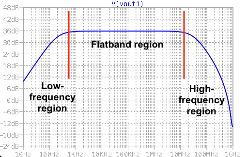
The Frequency response is shown above. There are three regions, low-frequency, flatband and high-frequency region. The low-frequency region is decided by C1, C2 and C3. C1 provides a low impedance path at high frequency. At high frequency, the gain starts dropping. The flatband region is the most useful region. In this region, the gain is the highest and remains constant over a wide range of frequencies. To analyze this region we can simplify the circuit further. C1, C2 and C3 can be as high as possible. Having them high allows us to simplify the above model as shown below:
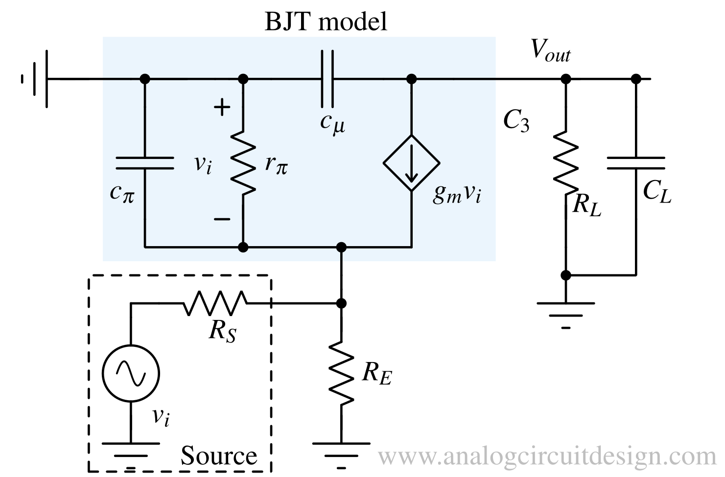
The above model ignores the low-frequency region and assumes the flatband starts from DC (0 Hz). It captures the flatband and high-frequency region. The -3dB bandwidth (fH) of the above circuit's transfer function (Vout/Vs) can be estimated :
$$f_H\simeq{}\cfrac{1}{2\pi{}(R_S||R_E||r_{\pi{}}||(1/g_m))c_{\pi}}$$
Due to absence of cμ, the bandwidth of CB amplifier is higher than CE amplifier.
Stability of the voltage gain across temperature
The voltage gain is directly proportional to the transconductance (gm) of the amplifier. The gm of the amplifier is inversly proportional to the temperture. If temperature increases, the gain falls.
$$\cfrac{V_o}{V_i}=g_mR_L=\cfrac{I_C}{V_t}R_L=\cfrac{I_C}{kT/q}R_L$$
$$\implies{}\cfrac{V_o}{V_i}\propto{}\cfrac{1}{T}$$
Cascode amplifiers
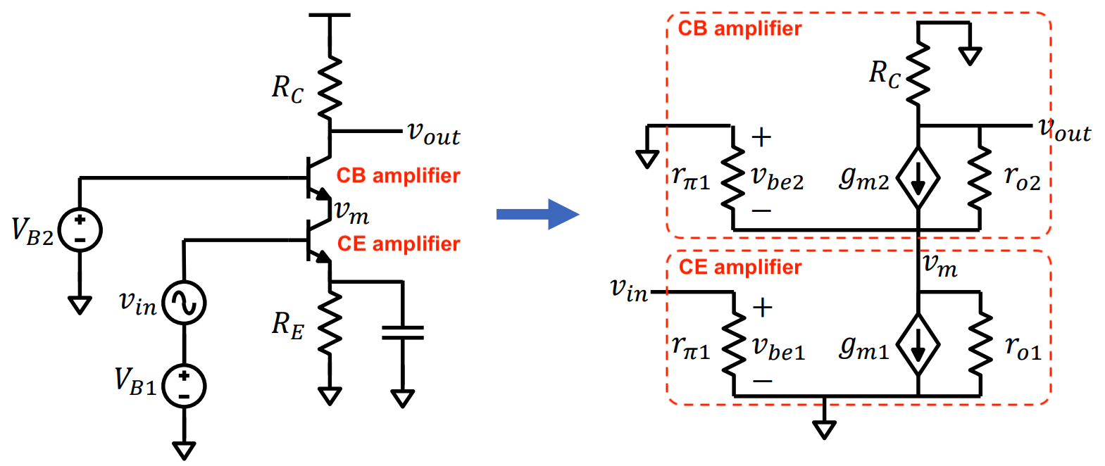
“Cascode” originates from “cascade of cathodes,” a term coined by early engineers. The first stage is a common-emitter (VCCS) stage and the second stage is common-base (CCCS) stage. So, it is also called CE-CB amplifier.
Input impedance : Rin = rπ
Output impedance : ro1ro2gm2. The output impedance is ro2gm2 times more than CE-amplifier's output impedance. This helps in achieving higher voltage gain.
Voltage gain : gm1(ro1ro2gm2||RC) ~ gm1RC