Common Collector Amplifier
The common-collector (CC) amplifier is a single transistor BJT amplifier with collector small signal grounded (i.e., constant DC voltage). Input terminal is base and output terminal is emitter. It behaves as a voltage controlled voltage source having gain of unity.
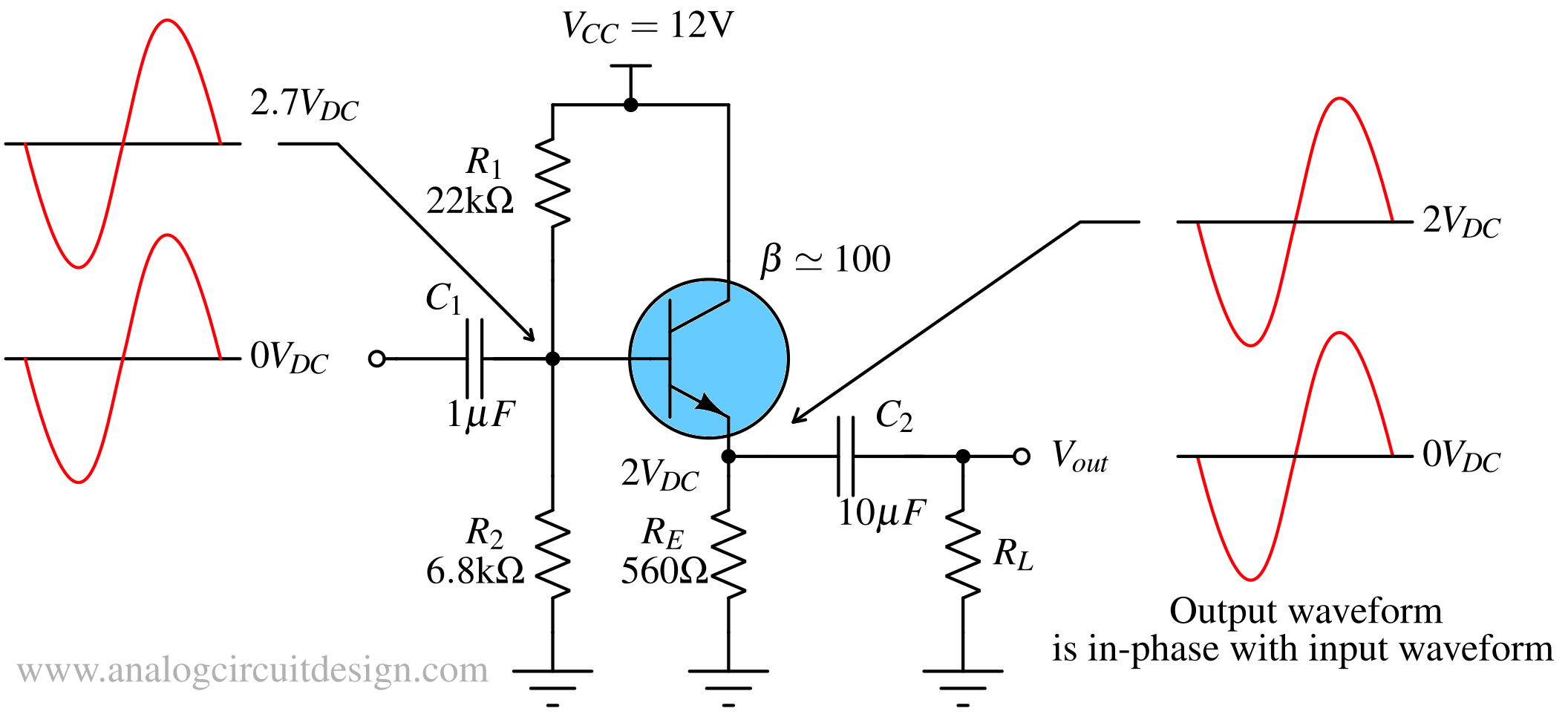
R1 & R2 are sets the DC bias of the transistor primarily. The value of R1 and R2 should be chosen such that the base current IB does not create significant voltage drop across R1||R2, otherwise VBE junction won't turn on.
RE sets the emitter and collector current of the amplifier. It also helps prevent excess current flowing through the VBE junction and prevents thermal run-away. The collector current establishes the gm (transconductance) of the BJT.
RC, RL and gm set the gain of the amplifier.
RL is the load resistor which emulates the input impedance of following stage. It is not strictly necessary for the operation of the amplifier. RL along with C3 ensures that the output will be at 0V when input is zero.
C1 is the input AC coupling capacitor. It allows input source to have difference DC bias voltage than the CC-amplifier.
C2 is the output AC coupling capacitor. It allows the input signal and the base voltage of the transistor to have different DC voltage.
Notice that the collector is directly connected to the supply voltage.
DC analysis
To get the DC operating points, the capacitors are replaced with open circuits in the above schematic.

The goal is to obtain the VCE voltage of the amplifier which gives us the maximum possible output voltage. Also, we need to find the value of collector current which will be used to find the transconductance (gm). To simplify the circuit, lets find the Thevenin equivalent circuit :
$$R_{TH}=\cfrac{R_1R_2}{R_1+R_2}=\cfrac{(6.8\,\text{k}\Omega{})\,(22\,\text{k}\Omega{})}{6.8\,\text{k}\Omega{}+22\,\text{k}\Omega{}}=5.19\,\text{k}\Omega{}$$
$$V_{TH}=\left(\cfrac{R_2}{R_1+R_2}\right)V_{CC}=\left(\cfrac{6.8\,\text{k}\Omega{}}{6.8\,\text{k}\Omega{}+22\,\text{k}\Omega{}}\right)12\,\text{V}=2.83\,\text{V}$$
KVL,
$$V_{TH}-I_BR_{TH}-V_{BE}-(I_C+I_B)R_E=0$$
Also,
$$I_C=\beta{}I_B$$
$$\implies{}V_{TH}-\cfrac{I_C}{\beta{}}R_{TH}-V_{BE}-I_C(1+\cfrac{1}{\beta{}})R_E=0$$
$$\implies{}I_C=\cfrac{V_{TH}-V_{BE}}{(R_{TH}+R_E)/\beta{}+R_E}\simeq{}3.58\,\text{mA}$$
Emitter Voltage,
$$V_E=I_ER_E=(3.58\,\text{mA})(560 \Omega{})=2.00\,\text{V}$$
Base voltage,
$$V_B=V_E+0.7\,\text{V}=2.70\,\text{V}$$
Collector-Emitter voltage,
$$V_{CE}=V_C-V_E=12-2=8\,\text{V}$$
The Collector-Emitter voltage should not be less than 200mV. Otherwise, the BJT will go into saturation and gain will be zero.
Small signal analysis
BJT like any other real transistor is a non-linear device. So it is converted into linear model called small-signal model as shown below. This model is not valid for DC however it is valid for flatband region and widely used in designing circuits. Beyond flatband region, we need to capture some more capacitors in the model which is shown in this section : Frequency response and bandwidth.
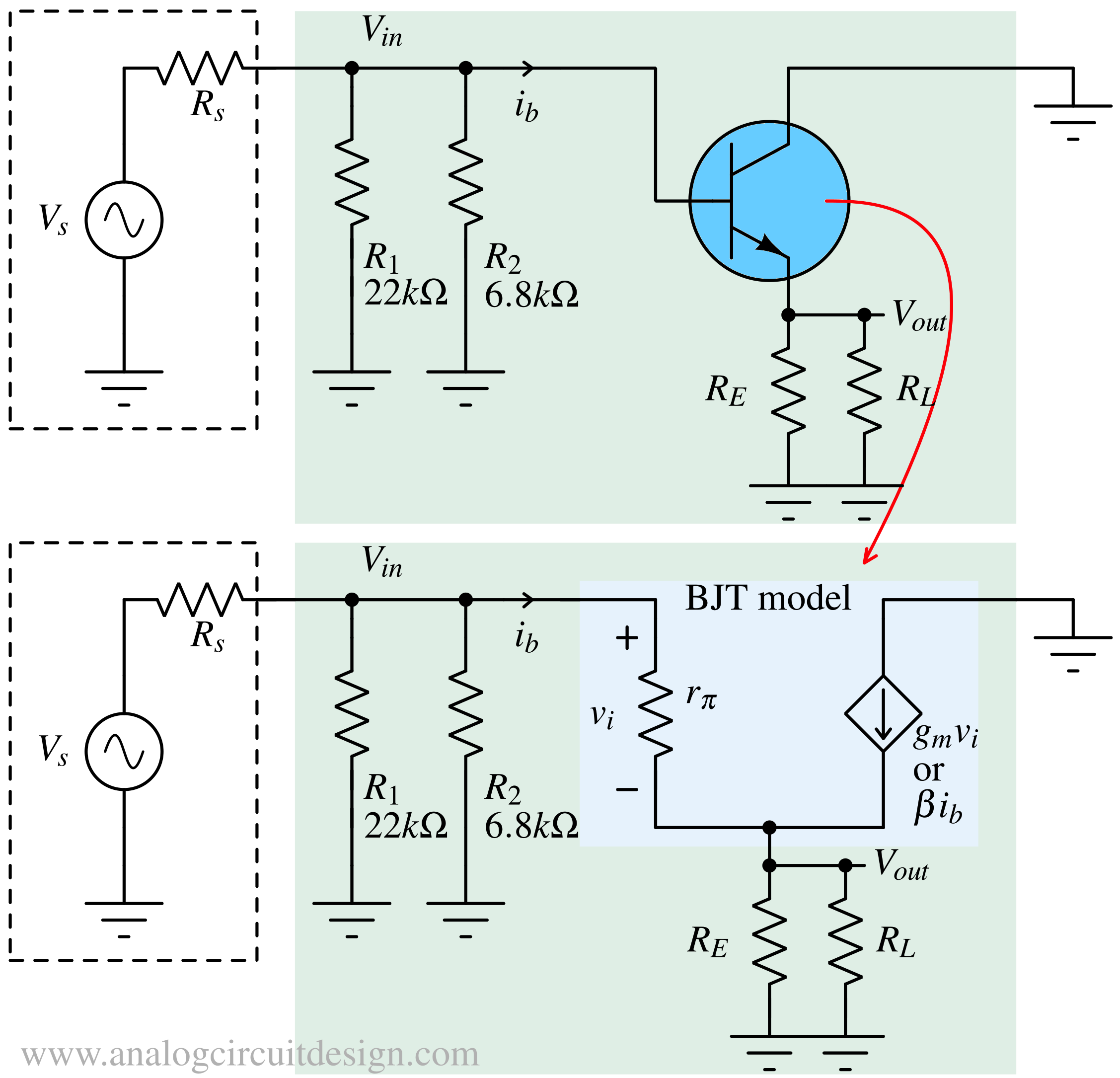
Transconductance
The transistor can be replaced by a transconductor and an input resistor. This model is applicable in any BJT configuration (Common-base, Common-collector, Common-emitter).
The transconductance gm is given by :
$$g_m=\cfrac{I_C}{V_T}$$
$$g_m=\cfrac{3.58\,\text{mA}}{25.6\,\text{mV}}=139\,\text{mS}$$
Input resistance
The input resistance of common collector amplifier is :
$$r_{in}=r_{\pi}+\beta{}(R_E||R_L)=\cfrac{\beta{}}{g_m}+\beta{}(R_E||R_L)$$
If RE=560Ω, RL=1kΩ, β=100 :
$$r_{in}=712\,\Omega{}+100\times{}358\,\Omega{}\simeq{}36.5\,\text{k}\Omega{}$$
Output resistance
The output resistance of common collector amplifier is :
$$r_{out}=r_{\pi}||\left(\cfrac{1}{g_m}\right)\simeq{}\cfrac{1}{g_m}$$
If gm=139mS :
$$r_{out}\simeq{}\cfrac{1}{139\,\text{mS}}=7.1\,\Omega{}$$
Voltage gain
The voltage gain can be calculated as :
$$A_v=\cfrac{v_o}{v_i}=\cfrac{g_m(R_E||R_L)}{1+g_m(R_E||R_L)}$$
If gm=139mS, RE=560Ω, RL=1kΩ :
$$A_v=\cfrac{g_m(R_E||R_L)}{1+g_m(R_E||R_L)}=\cfrac{139\times{}10^{-3}\times{}358}{1+139\times{}10^{-3}\times{}358}=\cfrac{49.76}{1+49.76}=0.98\,\text{V/V}$$
Current gain
Although the voltage gain is 1, the maximum current gain is β.
AC analysis
Frequency response and bandwidth
To analyze the frequency response of the common collector amplifier, we can use a more comprehensive small signal model of the BJT which includes parasitic capacitances as shown below (ro has been ignored for simplicity).
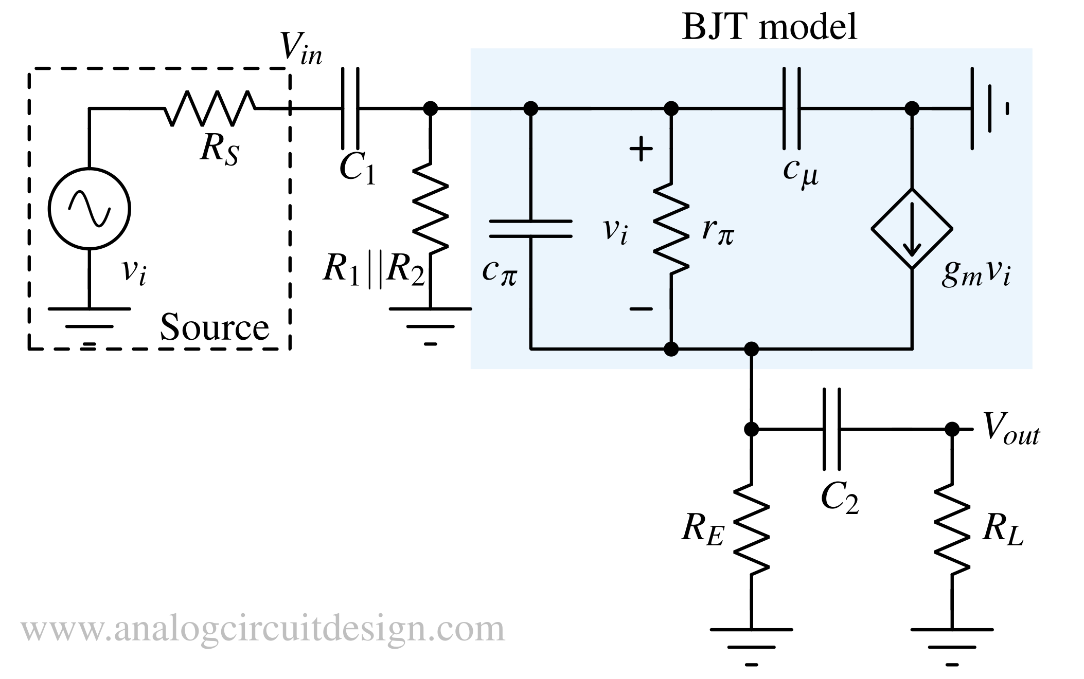
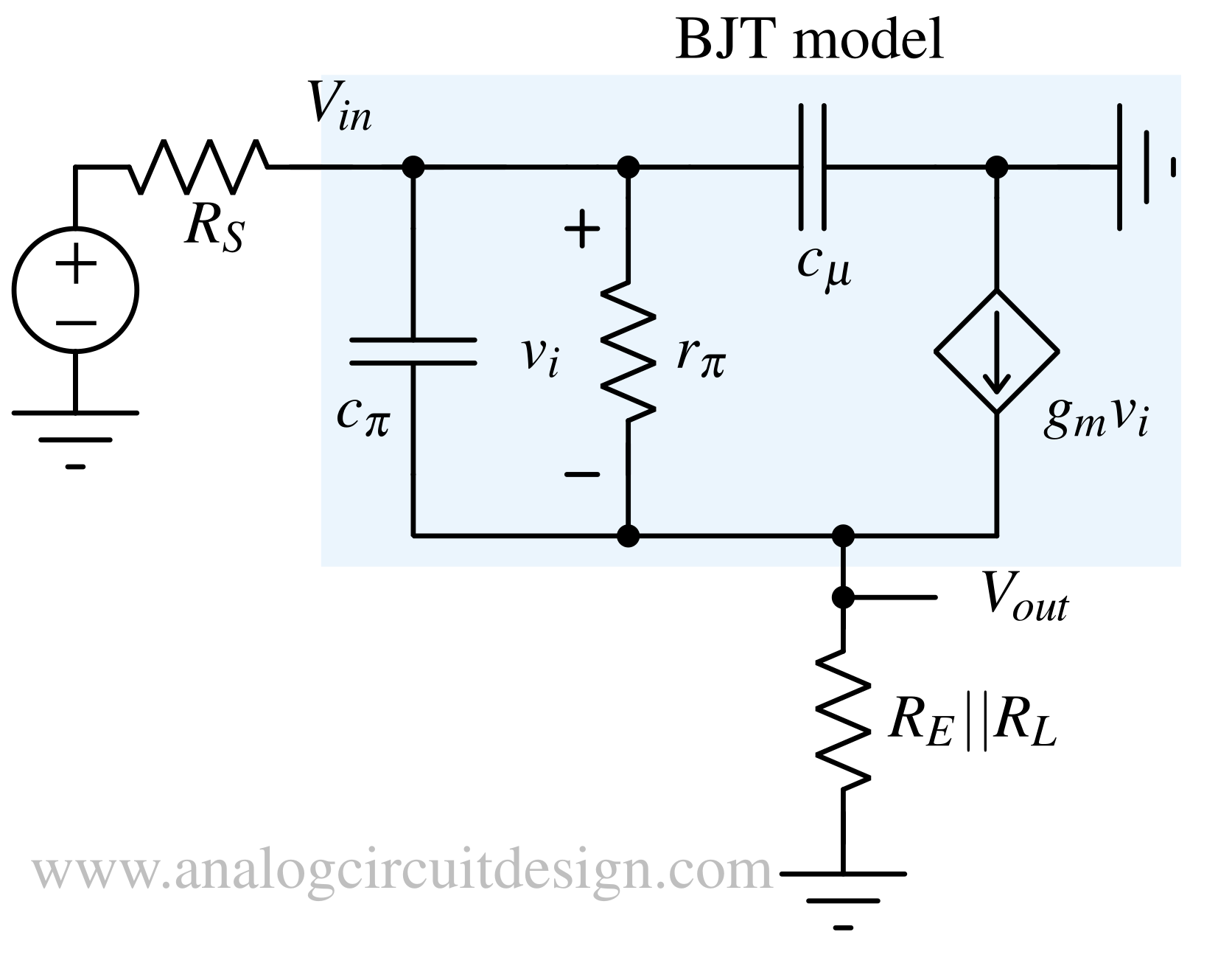
The Frequency response is shown above. There are three regions, low-frequency, flatband and high-frequency region. The low-frequency region is decided by C1, C2. C1 shorts the input and base of BJT at flatband and high frequency. At high frequency, the gain starts dropping. The flatband region is the most useful region. In this region, the gain is near unity and remains constant over a wide range of frequencies. To analyze this region we can simplify the circuit further. C1, C2 and C3 can be removed in the simplified model as they shorts the two nodes at flatband and high frequency
Effect of a Load on the Voltage Gain
The maximum voltage gain which can be obtained from a common collector amplifier is unity. With higher load, this gain falls below unity.
$$A_v=\cfrac{v_o}{v_i}=\cfrac{g_m(R_E||R_L)}{1+g_m(R_E||R_L)}$$
Usually gain greater than 0.9 is acceptable.
Darlington pair and Sziklai pair
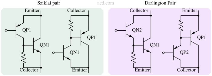
Darlington pair is a cascade of two common collector stages as shown above. It helps boost input impedance by β times. Sziklai-pair is a cascade of common-collector stage and a common-emitter stage as shown above. It lowers the output impedance by gmR.
Read more : Darlington and Sziklai pair
CC-CB compound transistor

CC-CB (Common-Collector + Common-Base) stage offers high input impedance with immunity to phase reversal. In this configuration, it behaves as a transconductor. The common collector's output impedance is low, so it is suitable to drive a common base's input. The input impedance of the common base is low. Since the same current flows through both the transistors, the individual transconductances are equal. This means the common collector's output impedance and the common base's input impedance are equal. This causes voltage division, so the voltage swing at the common point is only half of that of the input. Therefore current through this stage is vigm/2 instead of vigm.