Common Emitter Amplifier
Common-emitter amplifier is the simplest voltage gain amplifier. It uses a single transistor to achieve significant gain. The common-emitter (CE) amplifier is a single transistor BJT amplifier with emitter grounded. Input terminal is emitter and output terminal is collector. The emitter is common between input and output terminals. It behaves as a voltage controlled current source. The output current is passed through a resistive load to produce a voltage hence generating a voltage gain.
A common-emitter amplifier circuit is shown below :
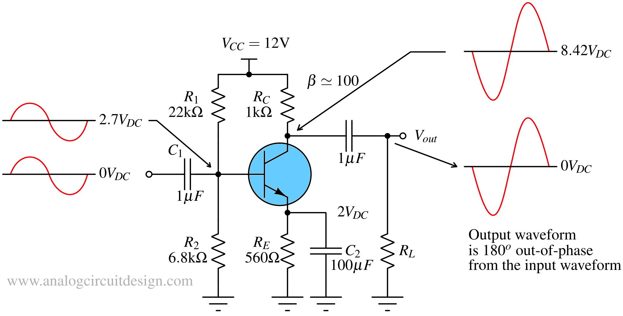
R1 & R2 are there to set the DC bias of the transistor primarily. The value of R1 and R2 should be chosen such that the base current IB does not create significant voltage drop across R1||R2, otherwise VBE junction won't turn on.
RE sets the emitter and collector current of the amplifier. It also helps prevent excess current flowing through the VBE junction and prevents thermal run-away. The collector current establishes the gm (transconductance) of the BJT.
RC, RL and gm set the gain of the amplifier.
RL is the load resistor which emulates the input impedance of following stage. It is not strictly necessary for the operation of the amplifier. RL along with C3 ensures that the output will be at 0V when input is zero.
C1 is the input AC coupling capacitor. It allows the input signal and the base voltage of the transistor to have different DC voltage.
C2 is the AC bypass capacitor. It bypasses RE at high frequency which increases the gain at high frequency. It does so by effectively grounding the emitter node.
DC analysis
To get the DC operating points, the capacitors are replaced with open circuits in the above schematic.
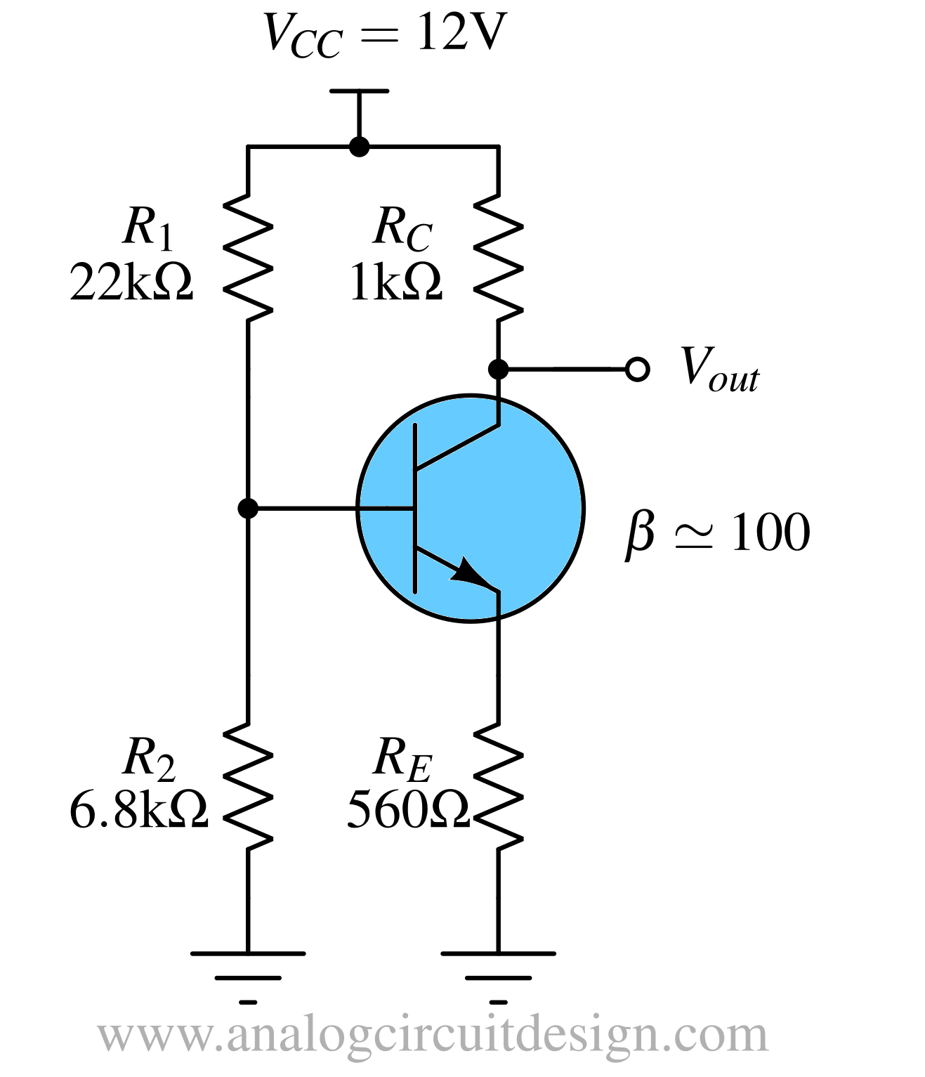
The goal is to obtain the VCE voltage of the amplifier which gives us the maximum possible output voltage. Also, we need to find the value of collector current which will be used to find the transconductance (gm). To simplify the circuit, lets find the Thevenin equivalent circuit :
$$R_{TH}=\cfrac{R_1R_2}{R_1+R_2}=\cfrac{(6.8\,\text{k}\Omega{})\,(22\,\text{k}\Omega{})}{6.8\,\text{k}\Omega{}+22\,\text{k}\Omega{}}=5.19\,\text{k}\Omega{}$$
$$V_{TH}=\left(\cfrac{R_2}{R_1+R_2}\right)V_{CC}=\left(\cfrac{6.8\,\text{k}\Omega{}}{6.8\,\text{k}\Omega{}+22\,\text{k}\Omega{}}\right)12\,\text{V}=2.83\,\text{V}$$
KVL,
$$V_{TH}-I_BR_{TH}-V_{BE}-(I_C+I_B)R_E=0$$
Also,
$$I_C=\beta{}I_B$$
$$\implies{}V_{TH}-\cfrac{I_C}{\beta{}}R_{TH}-V_{BE}-I_C(1+\cfrac{1}{\beta{}})R_E=0$$
$$\implies{}I_C=\cfrac{V_{TH}-V_{BE}}{(R_{TH}+R_E)/\beta{}+R_E}\simeq{}3.58\,\text{mA}$$
Emitter Voltage,
$$V_E=I_ER_E=(3.58\,\text{mA})(560 \Omega{})=2.00\,\text{V}$$
Base voltage,
$$V_B=V_E+0.7\,\text{V}=2.70\,\text{V}$$
Collector voltage,
$$V_C=V_{CC}-I_CR_C=12\,\text{V}-(3.58\,\text{mA})(1\,\text{k}\Omega{})=8.42\,\text{V}$$
Collector-Emitter voltage,
$$V_{CE}=V_C-V_E=8.42-2=6.42\,\text{V}$$
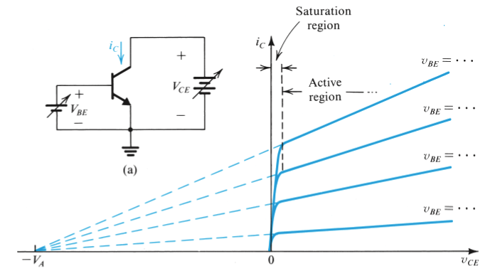
The Collector-Emitter voltage should not be less than 200mV. Otherwise, the BJT will go into saturation and gain will be zero.
Small signal analysis
BJT is a non-linear device. To simplify the analysis, a BJT is converted into linear model called small-signal model as shown below. This model is not valid for DC however it is valid for flatband region. The RE has been removed because there is C2 in parallel to it. This parallel combination of R and C reduces the impedance and effectively connects the emitter to ground at flat-band region. Beyond flatband region, we need to capture some more capacitors in the model which is shown in this section : Frequency response and bandwidth.

The model shown above is very useful to quickly calculate the gain of the circuit. To determine bandwidth of the circuit, we need small signal high-frequency model as it captures the internal capacitors of the BJT.
Transconductance
The transistor can be replaced by a transconductor at the output and input resistor at the input. This model is applicable in any BJT configuration (Common-base, Common-collector, Common-emitter).
The transconductance gm is given by :
$$g_m=\cfrac{I_C}{V_T}$$
$$g_m=\cfrac{3.58\,\text{mA}}{25.6\,\text{mV}}=139\,\text{mS}$$
Small signal input resistance
The small signal input resistance (looking into the base of the BJT) is denoted by rπ:
$$r_{\pi{}}=\cfrac{V_T}{I_B}$$
or
$$r_{\pi{}}=\cfrac{\beta{}}{g_m}$$
Assuming β=100,
$$r_{\pi{}}=\cfrac{100}{139\,\text{mS}}=715\,\Omega{}$$
Total input resistance
$$r_{in}=r_{\pi{}}||R_1||R_2$$
Due to presence R1 and R2, the input resistance decreases.
Small signal output resistance
The small signal output resistance is :
$$r_o=\cfrac{V_A}{I_C}$$
Where VA is the Early-voltage and IC is the collector current. If VA = 400V and IC = 3.58mA,
$$r_o=\cfrac{400\,\text{V}}{3.58\,\text{mA}}=111\,\text{k}\Omega{}$$
Small signal voltage gain
The output voltage (Vout) is :
$$V_{out}=-g_mv_iR_C$$
The voltage gain of the BJT in Common Emitter configuration alone is :
$$\cfrac{V_{out}}{v_i}=-g_mR_C$$
However, due to presence of source resistance (Rs) and load resistance (RL), the voltage gain drops. To calculate, lets find the effective input voltage. The input voltage (Vin or vi) is :
$$v_{i}=\cfrac{r_\pi{}||R_1||R_2}{r_\pi{}||R_1||R_2+R_s}V_s$$
Now the effective voltage gain can be denoted by :
$$\cfrac{V_{out}}{V_{x}}=-g_m(R_C||R_L)\cfrac{r_\pi{}||R_1||R_2}{r_\pi{}||R_1||R_2+R_s}$$
It can be observed that the voltage gain is dependent on source resistance Rs. If Rs is low, we get the high voltage gain which can come closer to the voltage gain obtained from a standalone common-emitter amplifier.
If RC,RL=1k, gm=139mS, and RS=0 we obtain:
$$\cfrac{V_o}{V_i}=g_m(R_C||R_L)=139\,\text{mS}\times{}(1000\,\Omega{}||1000\,\Omega{})=69.5\,\text{V/V} = 36.83\,\text{dB}$$
Small signal current gain
The ratio of current getting into the input terminal (base terminal) to the current coming out of the output terminal (collector terminal) is called the current gain : $$A_i = \cfrac{I_C}{I_B} = \beta{}$$
Power gain
CE amplifiers are widely used for voltage gains. They are rarely used for power gain (GP). So, power gain does not matter in CE-amplifier.
$$G_P=\cfrac{\text{Output Power}}{\text{Input Power}}=\cfrac{V_oI_o}{V_iI_i}$$
AC analysis
Frequency response and bandwidth
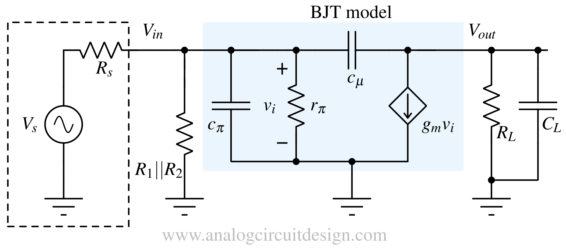
To analyze the frequency response of the common source amplifier, we can use a more comprehensive small signal model of the BJT as shown below.
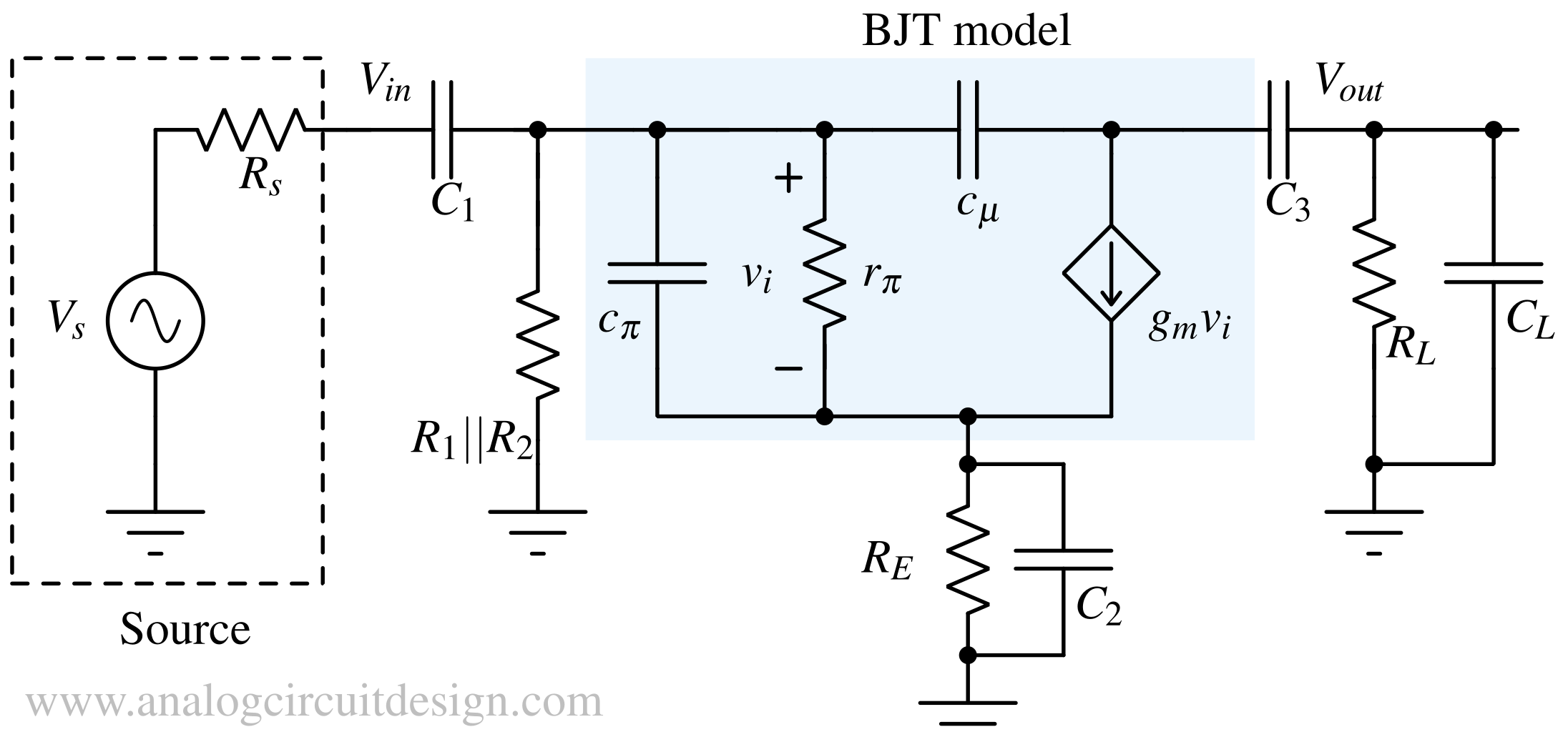
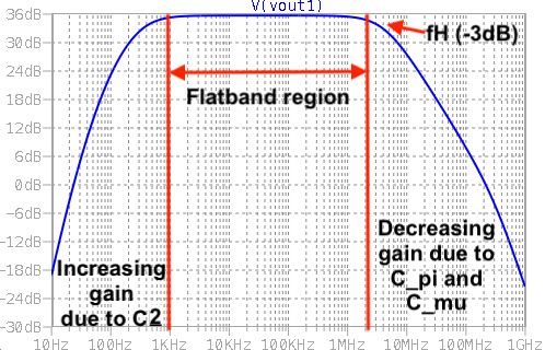
The Frequency response is shown above. There are three regions, low-frequency, flatband and high-frequency region. The low-frequency region is decided by C1, C2 and C3. The emitter-bypass capacitor C2 is a crucial capacitor to obtain high gain. The high frequency region tell us which component of our circuit is limiting the bandwidth. At high frequency, the gain starts dropping. The flatband region is the most useful region. In this region, the gain is the highest and remains constant over a wide range of frequencies. To analyze this region we can simplify the circuit further. C1, C2 and C3 can be as high as possible. Having them high allows us to simplify the above model as shown below:
The above model ignores the low-frequency region and assumes the flatband starts from DC. It captures the flatband and high-frequency region. The -3dB bandwidth (fH) of the above circuit's transfer function (Vout/Vs) can be estimated :
$$f_H\simeq{}\cfrac{1}{2\pi{}(R_1||R_2||R_s||r_{\pi})(c_{\pi}+c_{\mu}(1+g_mR_L))}$$
Due to Miller-multiplication of cμ, the effective input capacitance increases.
Effect of the Emitter Bypass Capacitor on Voltage Gain
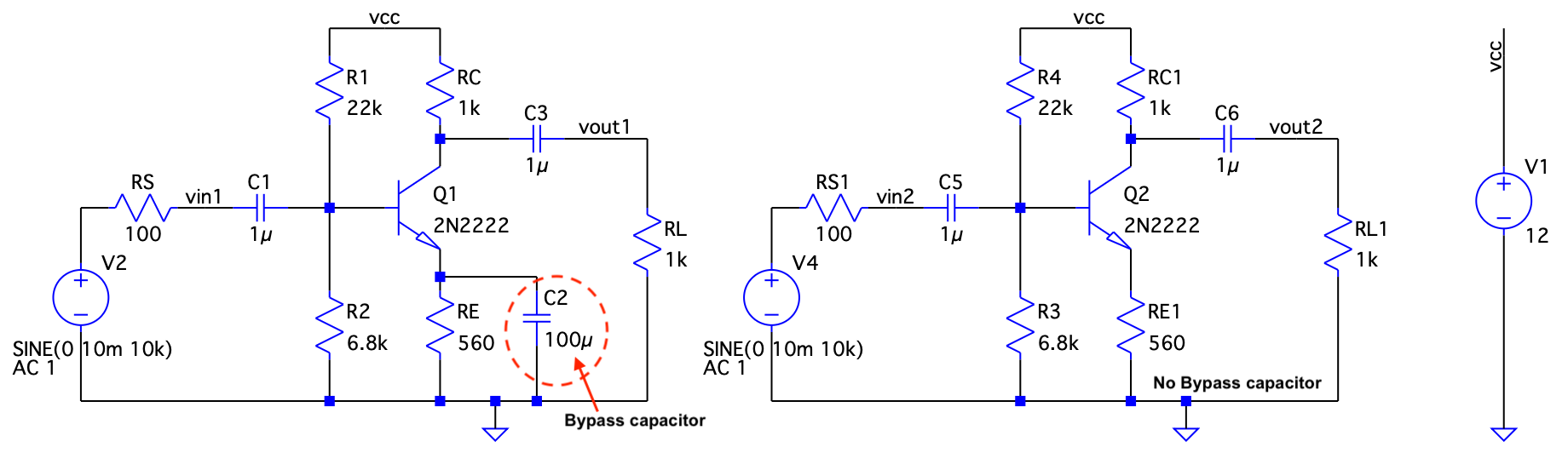
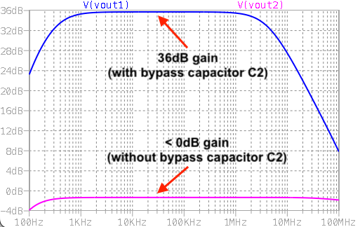
With bypass capacitor in parallel with RE, the voltage gain is significantly high. This is because at higher frequencies, the effective impedance (RE||1/sC2) drops. This increases the voltage appearing across the base-emitter terminal of the BJT. Without the bypass capacitor, the voltage gain is low as shown in above figure. Since, the impedance does not drop with frequency, the voltage swing at emitter-node is high. Therefore, the voltage across base-emitter junction is low; resulting in low gain.
Stability of the voltage gain across temperature
The voltage gain is directly proportional to the transconductance (gm) of the amplifier. The gm of the amplifier is inversly proportional to the temperture. If temperature increases, the gain falls.
$$\cfrac{V_o}{V_i}=g_mR_L=\cfrac{I_C}{V_t}R_L=\cfrac{I_C}{kT/q}R_L$$
$$\implies{}\cfrac{V_o}{V_i}\propto{}\cfrac{1}{T}$$
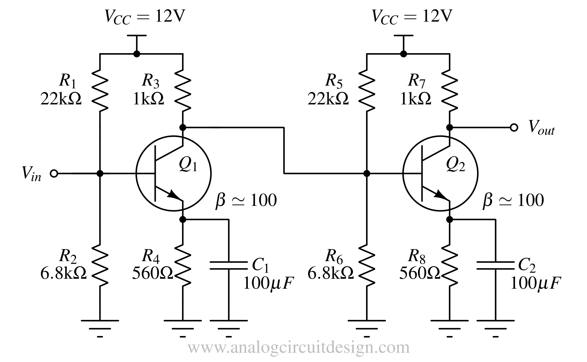
Capacitively Coupled Multistage Amplifier

Higher-gain can be achieved by using multiple common-emitter stages in cascade as shown above. The simplest method to cascade two CE amplifier stages is through capacitive coupling. The second stage's input loads the first stage's output which reduces the gain. However, overall gain can be made very high if this loading effect is minimised.
Loading Effects
The reduction in gain due to next stage's input circuit is called loading effect. In determining the voltage gain of the first stage, you must consider the loading effect of the second stage.
Voltage Gain of the First Stage
The voltage gain for the flatband region:
$$\cfrac{V_o}{V_i}=g_m(R_3||R_5||R_6||r_{\pi{},Q2})$$
If gm=139mS, R3=1kΩ, R5=22kΩ, R6=6.8kΩ and rπ,Q2=715Ω, using parallel resistor calculator, we find that :
$$R_3||R_5||R_6||r_{\pi{},Q2}=386\,\Omega{}$$
$$\cfrac{V_o}{V_i}=139\,\text{mS}\times{}386\,\Omega{}=53.65\,\text{V/V}=34.59\,\text{dB}$$
The gain achieved by the first stage with loading effect is 34.59 dB. Let's compare it with gain when the loading effect is not there.
$$\cfrac{V_o}{V_i}=g_mR_3=139\,\text{mS}\times{}1000\,\Omega{}=139\,\text{V/V}=42.86\,\text{dB}$$
The gain when there is no loading effect is 42.86 dB. So, loading effect reduced the gain by 8.27 dB.
Direct-Coupled Multistage Amplifiers
The CE-amplifier can be DC coupled as well. However, we have to be careful about the second stage's operating point influencing the first stage's operating point.