Digital to Analog Converters (DAC)
The process of conversion of a digital input signal (1s and 0s) into an analog output signal is called digital to analog conversion (D/A). The digital signal usually encoded using a binary code consisting of 0s and 1s. In electronics, the circuits and systems which help in converting the binary code into analog signals are called Digital to Analog Converters (DAC). These important in modern electronics because it enables the seamless conversion of digital signals, processed by digital systems, into analog signals that can interact with the real world.
Digital to Analog Conversion Calculator

Basic concept of DAC
Binary data is represented as voltage or current by assigning specific electrical levels to the two possible binary states (0 and 1), using a concept known as "logic levels." Typically, a "high" voltage (for example, +5V or +3.3V) represents binary 1, and a "low" voltage (for example, 0V or ground) represents binary 0. To generate something in-between +5V and 0V (for example, +2.33V), methods like voltage-division (e.g., R-2R ladder), current-addition (e.g., current-steering) are used.
Working principle of Digital to Analog Converter
The DAC accepts an n-bit digital input (a binary number). Each bit corresponds to a "weight" based on its position (e.g., bit 0 is worth 1, bit 1 is worth 2, bit 2 is worth 4, etc.). Each bit is associated with a scaled voltage or current contribution according to its binary weight. These weighted contributions are combined (summed) electrically, usually through a resistor network or current source arrangement. The summed result is an analog signal — a voltage or current — proportional to the numeric value of the digital input.
There are many ways to assign weight to a bit. In this example we will use inverting amplifier as summer to add different weights. We will scale resistors according to the weights they represent. In current switching/steering architecture, the current sources are scaled according to the bit they represent.

In above figure, a binary word (b3b2b1b0) is applied at the input. The output Vout is dependent on each input bit bi and resitor Ri. b3 is the MSB and b0 is the LSB. bi can assume value between 0 and Vref. To increase the contribution of b3 at the output, R3 can be reduced. To decrease the contribution of b0 at the output R0 can be increased. Also, when all the bits are turned-on, it should reflect the full-scale value Vref. The difference between adjacent code (e.g., 0011 and 0100) should be equal to 1-LSB (Vref/24).
The following circuit has all our requirements of a binary weighted DAC mentioned above:

The generalised equation of N-bit Binary weighted DAC (implemented as Fig 3) can be written as:
$$V_{DAC}=frac{V_{ref}}{2}\left(\cfrac{b_{N-1}}{2^{0}}+ \cfrac{b_{N-2}}{2^{1}}+dots{}+\cfrac{b_{0}}{2^{N-1}}\right)$$
Key specifications of Digital to Analog Converter
Resolution (N-bit)
Resolution determines the precision of a DAC. The greater the resolution, the finer outputs it can generate. The resolution is usually expressed as the number of bits (N) the DAC is using to create the analog output. For example, a DAC with an n-bit resolution has 2n possible digital codes which define 2n step levels. Resolution directly affects the perceived quality of both audio and video by determining how finely the continuous analog output can approximate the original signal. Higher resolution leads to smoother, more accurate reproduction, while low resolution introduces artifacts and distortion.
Least Significant Bit (LSB)
The least significant bit (LSB) represents the smallest voltage that can be generated by a one-bit change in the digital input.
$$\text{LSB}=\cfrac{V_{ref}}{2^N}$$
LSB is often used as the reference unit for other quantities in a DAC. In an ideal (reference) DAC, it can be understood as the smallest possible change in output voltage (or current) that can be produced by a one-bit change in the digital input. It is also a measure of the resolution of the converter since it defines the number of divisions or units of the full analog range.
Resolution and LSB for Vref = 4.096V [1]
| Resolution | LSB |
|---|---|
| 8-bit | 16.00mV |
| 10-bit | 4.00mV |
| 12-bit | 1.00mV |
| 14-bit | 250uV |
| 16-bit | 62.5uV |
Quantisation levels
In a digital-to-analog converter (DAC), quantization levels refer to the number of discrete voltage (or current) values that the DAC can output (like the steps in a ladder). Each (Voltage/Current) level corresponds to a unique binary code at the input of the DAC. The number of these levels is directly related to the DAC's resolution, which is typically specified in bits. A higher number of bits means more quantization levels and, therefore, a finer approximation of the input digital signal.
Resolution and Quantisation levels
| Resolution | Quantisation levels |
|---|---|
| 8-bit | 256 |
| 10-bit | 1024 |
| 12-bit | 4096 |
| 14-bit | 16384 |
| 16-bit | 65536 |
Quantization error
Quantization error is the difference between the ideal expected analog signal and the closest available analog voltage produced by the DAC. This error arises because a DAC can only output a limited number of discrete analog values, so when converting a digital code, it "rounds" to the closest possible output level—introducing a small discrepancy from the theoretically exact value. Quantization error happens for a ideal DAC as well. For an ideal N-bit DAC, this error is always within ±½ Least Significant Bit (LSB) of the intended analog value. Quantization error is modelled as a noise on the output, called quantization noise, and sets a fundamental limit to the accuracy of signal reconstruction.
Full scale output
The full-scale (FS) output of a digital-to-analog converter (DAC) is the maximum analog output signal that the DAC can produce in response to the highest possible digital input code. It is typically defined as the analog output corresponding to the largest input code the DAC is capable of receiving (usually all input bits set to 1) and is determined by the reference voltage and the architecture of the DAC.
$$\text{FS}=V_{ref}\cfrac{2^n-1}{2^n}$$
For a 10-bit DAC with Vref = 3.3V,
$$\text{FS}=3.3\cfrac{2^{10}-1}{2^{10}}=3.296,\text{V}$$
Settling time
Settling time in a DAC (digital-to-analog converter) is the amount of time required for the output to transition from one value to another (due to a change in digital input) and remain within a specified error band - typically ±(1/2) LSB - of its final value. Settling time starts at the moment the digital input is changed and includes all transient behaviours such as propagation delay, slewing, overshoot, undershoot, and ringing. It ends when the output no longer leaves the specified error band (e.g., ±½ LSB or ±0.01% of full scale) around its intended final value
Sampling rate
The sampling rate in a digital-to-analog converter (DAC) is the number of digital data points (samples) per second that the DAC converts into corresponding analog voltage or current signals. It is typically expressed in samples per second (SPS) or Hertz (Hz), where 1 Hz = 1 SPS. According to Nyquist-Shannon’s Sampling Theorem, to accurately reconstruct a signal with a maximum frequency fmax, the DAC must be supplied digital samples at a rate of at least twice that frequency (the Nyquist rate : fs > 2fmax) to avoid aliasing distortion.
Differential Non-Linearity (DNL)
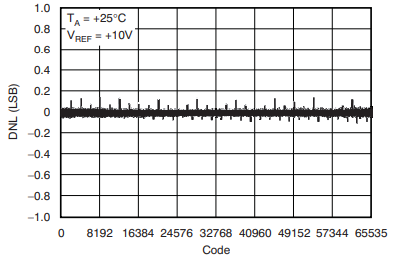
Differential Non-Linearity (DNL) is a measure of how much the step size between consecutive analog output levels deviates from the ideal value (which should be exactly 1 Least Significant Bit, LSB). In an ideal DAC, increasing the digital input code by 1 always increases the analog output by 1 LSB. DNL can be defined for every step however while reporting DNL of a DAC, the worst case is quoted.
$$\text{DNL}=\cfrac{V(D+1)-V(D)}{V_{LSB,ideal}}-1$$
Where,
$$0<D<2^{N}-2$$
$$V_{LSB,ideal}=\cfrac{V_{ref}}{2^N}$$
V(D) is the analog value represented by the digital code D, V(D+1) is the analog voltage corresponding to the next code. N is the DAC's resolution, and VLSB,ideal is the ideal LSB for a N-bit DAC.
Some key points to note about DNL of a DAC:
- Ideal case: DNL = 0 LSB for every step (all steps are uniform).
- Positive/negative DNL: A step larger than 1 LSB has positive DNL, while one smaller than 1 LSB (but not missing entirely) has negative DNL.
- DNL > 1 LSB: Implies missing codes—some digital input codes do not produce a unique output level.
- DNL < -1 LSB: May cause non-monotonic output, meaning the analog output could decrease for an increase in input—a highly undesirable property for control systems
Integral Non-Linearity (INL)

Integral Non-Linearity (INL) is a measure of the deviation of the actual DAC transfer function from an ideal straight line. This ideal line can be drawn using either endpoint-fit (straight line from minimum to maximum output) or best-fit methods.
INL at any code is the difference between the actual output and the ideal output (from the reference line) at that code, after offset and gain errors have been removed.
$$\text{INL}=\cfrac{V(D)-V(0)}{V_{LSB,ideal}}-D$$
Where,
$$0<D<2^{N}-1$$
$$V_{LSB,ideal}=\cfrac{V_{ref}}{2^N}$$
V(D) is the analog value represented by the digital output code D, N is the DAC's resolution, V(0) is the minimum analog input corresponding to an all-zero input code, and VLSB,ideal is the ideal LSB for a N-bit DAC.
INL accumulates the net errors of all previous DNL errors up to a given code. It is reported as the worst-case (maximum) deviation for all codes, usually in LSBs or as a percentage of full scale.
Offset error

Offset error is the constant difference between the actual output and the ideal output at zero digital input. In other words, when the digital input code is zero, the DAC's output voltage (or current) is not exactly zero due to this error.
This shifts the entire DAC transfer function vertically (as shown in above figure), causing all output values to be offset by a fixed amount. The ideal DAC transfer function can be described by the linear equation “y=mx+c”, where “y” is the output voltage, “x” is the digital input, “m” is the gain (slope), and “c” is the offset error (y-intercept). This error reduces the effective output range and can be corrected by calibration or software compensation.
Gain error

Gain error is the deviation of the actual output slope from the ideal output slope of the DAC’s transfer function after offset error is removed. It represents a scaling error (as shown above) where the output voltage or current is either stretched or compressed compared to the ideal linear response, causing the output range to be inaccurately scaled. In practical terms, gain error causes the output to saturate too early or reach a lower-than-expected maximum.
Monotonicity
Monotonicity in a digital-to-analog converter (DAC) means that the analog output never decreases as the digital input code increases—in other words, each increment in the digital input either leaves the output unchanged or increases it, but never causes it to decrease. This property is critical for control applications and feedback systems, where a non-monotonic DAC could drive the system in positive feedback causing instability or oscillation.
DNL's impact on monotonicity
A DAC is guaranteed to be monotonic if its DNL error is greater than -1 LSB for every step. If DNL falls below -1 LSB at any step, the output at that step can decrease compared to the previous step, causing non-monotonic behaviour and potentially missing codes (levels). Thus, maintaining DNL > -1 LSB ensures monotonicity without missing codes.
INL's impact on monotonicity
While INL is less directly related to monotonicity than DNL, a small INL error (typically less than ±0.5 LSB) generally helps ensure monotonicity. If INL is large, it can lead to greater nonlinear distortion but will not necessarily break monotonicity if DNL criteria are met. Conversely, monotonicity does not guarantee a low INL value.
Missing codes
A missing code in a digital-to-analog converter (DAC) refers to a situation where at least one digital input value does not produce a corresponding unique analog output level. In other words, when the digital input is swept across all possible codes, there are some input codes for which the DAC output never transitions to a unique new level—effectively "skipping" those codes entirely.
Total Harmonic Distortion of a DAC
THD is the ratio of the sum of the powers of all harmonic frequency components (such as 2nd, 3rd, etc.) to the power of the fundamental frequency, generally expressed as a percentage or in decibels (dB).
$$\text{THD}=20log_{10}\left(\cfrac{\sqrt{V_2^2+V_3^2+V_4^2}}{V_1}\right)$$
In a DAC, non-idealities such as resistor or current source mismatch, output op-amp nonlinearity, and other imperfections generate additional harmonic signals at integer multiples of the input (fundamental) frequency.
Common noise sources in a DAC
- Internal DAC resistors: Thermal noise from the DAC's internal resistor strings (string DACs, R-2R DACs, MDACs).
- Output amplifier or buffer noise: The output amplifier after the DAC core generates noise such as broadband thermal noise (flat-band noise) and low-frequency 1/f noise.
- Current noise of the current sources: In Current steering DACs used for high speed applications, the current sources add thermal noise at the output.
- Voltage reference noise: The precision voltage reference (Vref) used by the DAC to set output voltage levels introduces noise.
- Quantization noise: This type of noise is intrinsic to the digital-to-analog conversion process. It results from the finite resolution (number of bits) of the DAC, causing small errors in representing the analog output. Quantization noise is related to the DAC's resolution and appears as a low-level noise component.
- Clock jitter and digital interface noise: The timing jitter of the digital clock feeding the DAC and noise coming through digital input signals can cause output fluctuations, including phase noise in high-speed DACs.
- Power supply noise: Fluctuations and noise in the DC power supplies feeding the DAC circuitry can couple into the output, causing output noise and distortion.
- External electromagnetic interference (EMI) and radio frequency interference (RFI): Noise picked up from the environment due to poor shielding or PCB layout can interfere with the DAC signals
Types of Digital to analog converters
Some of the DAC types are listed below:
- Binary weighted DAC
- R-2R ladder DAC
- Pulse-width modulation (PWM) DAC
- Delta-Sigma Modulated DAC or Oversampling DAC
- String DAC or thermometer coded DAC
- Current switching/steering DAC
- Switched capacitor DAC
Digital to Analog Converter ICs
Some available Digital to Analog Converter ICs are listed below :
| IC name | Architecture | Resolution | Max sampling speed | Manufacturer |
|---|---|---|---|---|
| AD558 | R-2R | 8-bit | 1 MSPS | Analog Devices |
| DAC0808 | R-2R | 8-bit | 6.6 MSPS | Texas Instruments |
| AD9739A | Current-steering | 14-bit | 2.5 GSPS | Analog Devices |
| DAC38RF82 | Current-steering | 14-bit | 9 GSPS | Texas Instruments |
| AD5620 | String | 12-bit | 125 KSPS | Analog Devices |
| MCP4725 | String | 12-bit | 6 KSPS | Microchip |
| TLV5630 | String | 12-bit | 283 KSPS | Texas Instruments |
| DAC8820 | MDAC | 16-bit | 2 MSPS | Texas Instruments |
| AD5543 | MDAC | 16-bit | 2.47 MSPS | Analog Devices |
References
[1] LTC6652