JK Latch and JK flip-flop
The JK Latch represents an advancement over the SR Latch by resolving the forbidden state issue inherent in the SR Latch through the inclusion of feedback. In a NAND gate-based J K latch, the feedback is taken from the output Q and Q and connected at the input NAND gate along with J, K and CLK.
The JK Latch/Flip-Flop, originally named after its inventor, Jack Kilby, who pioneered the integrated circuit in 1958.
J-K latches refer to level-triggered J-K flip-flops, distinguishing them from edge-triggered J-K flip-flops. Level-triggered devices are termed latches, while their edge-triggered counterparts are called flip-flops.
J K latch using NAND gate
J K latch using NAND gate is similar to gated S R Latch using NAND gates. We have two input NAND gates and two output NAND gates. The two output NAND gates are connected in a cross-coupled configuration forming a S R Latch. Q is connected to the input NAND gate where K is connected. Q is connected to input NAND gate where J is connected.

Truth Table of J K Latch
Table : Truth table of Falling-edge triggered J K flip flop
| Trigger | Inputs | Output | Note | ||||
|---|---|---|---|---|---|---|---|
| Present state | Next state | ||||||
| CLK | J | K | Qn | Qn+1 | |||
| 0 | X | X | X | Q | RETAIN | ||
| 1 | 0 | 0 | 0 | 0 | RETAIN | ||
| 1 | 0 | 0 | 1 | 1 | RETAIN | ||
| 1 | 0 | 1 | 0 | 0 | RESET | ||
| 1 | 0 | 1 | 1 | 0 | RESET | ||
| 1 | 1 | 0 | 0 | 1 | SET | ||
| 1 | 1 | 0 | 1 | 1 | SET | ||
| 1 | 1 | 1 | 0 | 1 | TOGGLE | ||
| 1 | 1 | 1 | 1 | 0 | TOGGLE |
When both J and K inputs are 0, the latch holds its state (Qn+1 = Qn). When J is 0 and K is 1, the latch resets (Qn+1 = 0). When J is 1 and K is 0, the latch sets (Qn+1 = 1). When both J and K are 1, the latch toggles (Qn+1 = Qn).
Working of J K Latch
We will understand the workings of J K latch by simplifying each case and get an intuitive understanding.
When CLK=1, the input to the internal latch is allowed to change. If CLK=0, both the input to the internal latch is 1 (as shown in Fig 2), which is RETAIN state in the S R latch using NAND gates.

When J and K are both 0, the latch maintains its previous state (it holds Q). This is because, the input to the internal latch is 1 and according to the truth table of the SR latch using NAND gates, it is a RETAIN state.

When J is 0 and K is 1, the latch resets to 0 (Q = 0, Q = 1). To understand this, we can replace the top left 3-input NAND gate with logic 1. This is because one of the inputs is 0, forcing the NAND output to be 1. The bottom left NAND gate can be replaced with an inverter because other inputs are 1. If Q is 1, the output of the inverter is 0, and the input of the bottom right NAND gate is 0. This forces Q = 1 and Q = 0. This is a RESET state. If Q is 0, the output of the inverter is 1, and the input of the bottom right NAND gate is 1. This retains the previous state of Q = 0 and Q = 1 which is nothing but RESET state again.

When J is 1 and K is 0, the latch sets to 1 (Q = 1, Q = 0). To understand this, we can replace the top left 3-input NAND gate with an inverter and the bottom left NAND gate can be replaced with logic 1.
If Q is 1, the output of the inverter is 0, and the input of the top right NAND gate is 0. This forces Q = 1 and Q = 0. This is a SET state.
If Q is 0, the output of the inverter is 1, and the input of the top right NAND gate is 1. This retains the previous state of Q = 0 and Q = 1 which is nothing but SET state again.

When both J and K are 1, it toggles its previous state (Qn+1 =Qn). To make the understanding simple, the 3-input NAND gates (from the J K latch schematic) can be replaced with NOT gates as shown in Fig 5.
If Q=1 and Q=0 (a SET state), the output of the top left inverter is 1, and the output of the bottom left inverter is 0. The latch goes into the RESET state.
When in RESET state, Q=0 and Q=1, the output of the top left inverter is 0, and the output of the bottom left inverter is 1. The latch goes into the SET state again.
We can see that the state is toggling between SET and RESET state. So, it is called TOGGLE state.
J K latch using NOR gate

J K latch can be built using NOR gates also (as shown in Fig 6). It is made using NOR-gate-based SR Latch and three-input AND gates at the input. Feedback is taken from the output to the input in a similar way as in NAND-based implementation (shown in Fig 1).
Race condition in J K Latch
The JK latch addresses the issue of both inputs being '1' (forbidden) in the SR latch by employing feedback connections from output to input. This helps eliminate the forbidden condition; however, the scenario when both J and K equal '1' (level triggered) is still prone to one problem called a race condition.
In the last state (TOGGLE state), if we refer to Fig 5, we see that the change of state can continue without stopping in cases where J, K, and CLK are all simultaneously high. The continuous change of state happens at the rate of the propagation delay of each gate leading to oscillations. This undesirable oscillation is called race condition in the J K latch.
Race condition intuitively means that two signal races against each other to decide the output of a logic gate. To solve the race condition from latches, flip-flops are used as mentioned in the J K flip-flop section. In flip-flops, most of the time, the feedback is broken and connected only during clock edges.
J K flip flop circuit diagram
J K flip-flop can be constructed using J K latches in the master-slave configuration, as shown below. It can be made using NOR gates or exclusively with NAND gates.
J K flip flop using NOR gates

An edge-triggered J-K flip-flop can be made using NOR gate-based J-K latches. Two latches can be connected in master-slave configuration to create a J-K flip-flop.
J K Flip Flop using NAND gates

Similarly, NAND gate-based J-K flip-flop can be made using two NAND gate-based J-K latches in a master-slave configuration.
J K flip flop working
Let’s take the example of the J K flip-flop we have in Fig 8.
When CLK = 1, the latch-1 (master latch) is activated while latch-2 (slave latch) is deactivated. This means that J and K signals can now change the state of the latch-1, however, the internal state of the latch-2 cannot be changed. If J = 1, K = 0 the output of the latch-1 is 1 (Q=1). However, it does not affect the state of the latch 2.
As soon as the CLK = 0, latch-1 deactivates and latch-2 is activated. The latch-2 captures the output of latch-1 while latch-1 RETAIN the state it had when CLK was 1. The output of latch-1 was Q=1 (and Q = 0) so, the input to latch 2 is again S = 1 and R = 0. Hence the output of latch-2 is again Q = 1. Since the latch-1 is disabled, nothing can enter this flip-flop.
When CLK = 1 again, the latch-1 is enabled while latch-2 is disabled again. Since the latch-2 is disabled, the latch-2’s state is unchanged while latch-1 can change its state.
Why race condition in J K flip flop does not exist?
J K flip-flops are constructed using master-slave topology. In the case where race-condition can happen (J=K=1), one of master or slave is turned-off which cut-off the path of racing condition. The only time when both master and slave are probably turned-on is the edge duration which is very small duration in-terms of the propagation delay of the race path.
J K flip flop truth table
A negative edge J K flip-flop's truth table in mentioned below:
Table : Truth table of Falling-edge triggered J K flip flop
| Trigger | Inputs | Output | Note | ||||
|---|---|---|---|---|---|---|---|
| Present state | Next state | ||||||
| CLK | J | K | Q | Qn | |||
| Not - ↓ | X | X | X | X | RETAIN | ||
| ↓ | 0 | 0 | 0 | 0 | RETAIN | ||
| ↓ | 0 | 0 | 1 | 1 | RETAIN | ||
| ↓ | 0 | 1 | 0 | 0 | RESET | ||
| ↓ | 0 | 1 | 1 | 0 | RESET | ||
| ↓ | 1 | 0 | 0 | 1 | SET | ||
| ↓ | 1 | 0 | 1 | 1 | SET | ||
| ↓ | 1 | 1 | 0 | 1 | TOGGLE | ||
| ↓ | 1 | 1 | 1 | 0 | TOGGLE |
The truth table of J K Flip flop is mentioned in the above table. The condensed form to express the Qn (next state) in terms of Q (present state), J and K (present inputs) is: $$Q_n=J\overline{Q}+\overline{K}Q$$
J K flip flop excitation table
Table : Excitation table of J K flip flop
| Qn | Qn+1 | J | K |
|---|---|---|---|
| 0 | 0 | 0 | X |
| 0 | 1 | 1 | 0 |
| 1 | 0 | X | 1 |
| 1 | 1 | X | 0 |
J K flip flop verilog code
Verilog code (behavioural model) of a positive edge triggered J K flip flop is written below. The synthesis will use a D flip flop to store the logic.
module jk_ff ( input j, input k, input clk, output q, output q_b);
reg q;
always @ (posedge clk)
case ({j,k})
2'b00 :  q <= q;
2'b01 :  q <= 0;
2'b10 :  q <= 1;
2'b11 :  q <= ~q;
endcase
assign q_b = ~q; endmodule
J K flip flop timing diagram
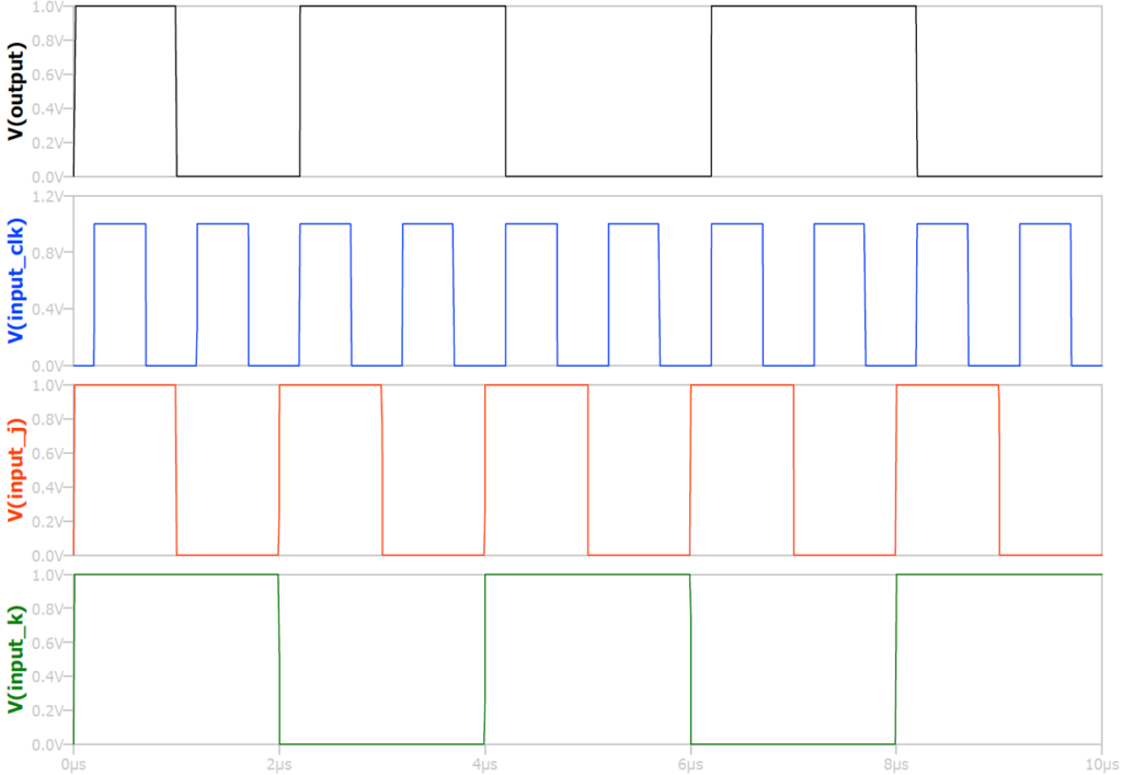
The timing diagram of a positive (rising) edge triggered J K flip-flop is shown in above figure.