MOSFET Parasitic Capacitance
Delay of digital CMOS circuits depends of capacitance of MOS device. There is a trade off between parasitic capacitance and drive strength of MOS device. Larger Cox increases the drive strength (IDS equation). However, larger Cox increases the device parasitic capacitance. Between almost every two terminals of MOS device, there is a source of parasitic capacitance.
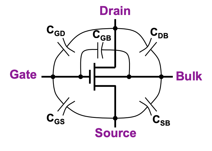
$$C_{GS}=C_{GSCH}+C_{GSOV}$$
$$C_{GD}=C_{GDCH}+C_{GDOV}$$
$$C_{GB}=C_{GBCH}$$
$$C_{SB}=C_{Sdep}$$
$$C_{DB}=C_{Ddep}$$
MOS parasitic capacitance types
A MOSFET has following parasitic capacitance types :
- Overlap capacitance
- Channel capacitance
- Junction capacitance
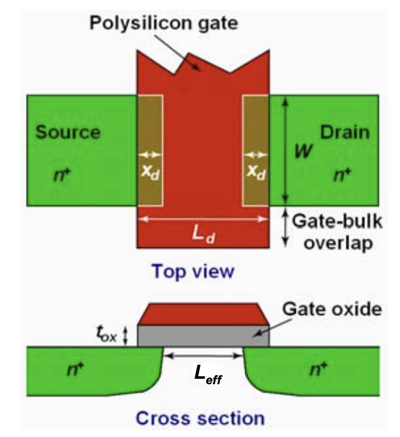
Overlap capacitance
Because of the lateral S/D diffusion, there is an overlap between gate and S/D junctions. This overlap capacitance is a constant linear capacitance.
$$C_{GSOV}=C_{GDOV}=WC_{ox}X_d$$
Channel Capacitance
Channel capacitance is a voltage dependent and non-linear capacitance.
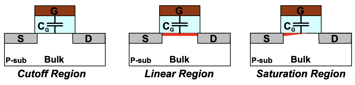
| Operating Region | CGBCH | CGSCH | CGDCH |
|---|---|---|---|
| Cutoff | CoxWLeff | 0 | 0 |
| Linear | 0 | 0.5CoxWLeff | 0.5CoxWLeff |
| Saturation | 0 | (2/3)CoxWLeff | 0 |
Junction Capacitance
Junction capacitance is the depletion region capacitance of source and drain. It is a voltage dependent capacitance (reverse biased pn-junction diode).
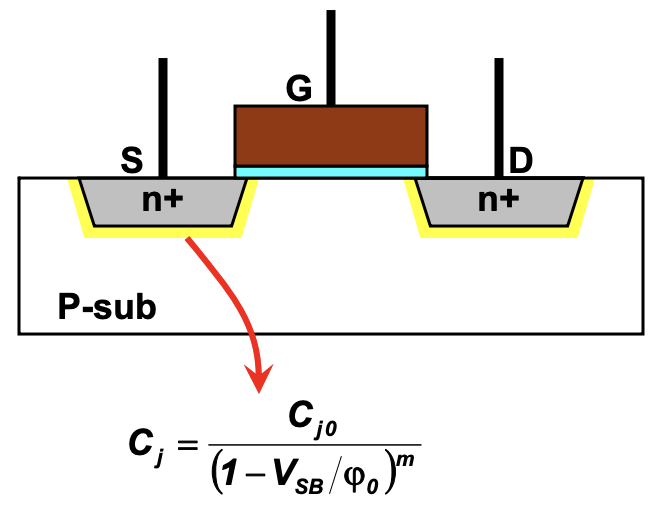
$$C_j=\cfrac{C_{j0}}{\left(1-\cfrac{V_{SB}}{\phi{}_0}\right)^m}$$
$$C_{j0}=A_D\sqrt{\left(\cfrac{\epsilon{}_{si}q}{2}\cfrac{N_AN_D}{N_A+N_D}\right)\phi{}_0^{-1}}$$
$$\phi{}_0=\cfrac{kT}{q}\ln{\cfrac{N_AN_D}{n_i^2}}$$
Junction Capacitance Components
Total junction capacitance can be partitioned into bottom junction and side-wall junction capacitors. The gate edge is often ignored since it is part of the conducting channel. Both source and drain have bottom and side-wall junction capacitance.
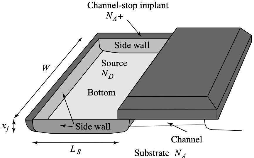
$$C_{dep}=C_{bottom}+C_{SW}$$
$$C_{bottom}=C_{jbottom}WL_s$$
$$C_{SW}=C_{jSW}(2L_s+W)$$