Noise in electronic circuits
Electronic noise is the unwanted, random fluctuation in electrical signals, voltages, or currents present in all electronic circuits. Noise sets minimum signal level which can be detected. It directly trades with power dissipation and bandwidth.
Signal-to-noise ratio (SNR)
Signal-to-Noise Ratio (SNR or S/N) measures the strength of a desired signal relative to background noise in a communication channel, engineering system, or data set, typically expressed in decibels (dB). A higher SNR indicates better quality, meaning more useful information (signal) and less interference.
$$\text{SNR}=\cfrac{P_{signal}}{P_{noise}}$$
Because signal levels can vary order of magnitudes, SNR is often expressed in decibels:
$$\text{SNR}_{dB}=10\log_{10}\left(\cfrac{P_{signal}}{P_{noise}}\right)$$
Noise figure (NF)
Noise figure (NF) is a measure of how much an electronic component or system (e.g.,amplifier, receiver) degrades the signal-to-noise ratio (SNR) as a signal passes through it. Expressed in decibels (dB), it is the ratio of input SNR to output SNR, with a lower value indicating better performance.
More about SNR and Noise figure : SNR and Noise Figure
Time-Domain Noise Concepts
Instantaneous noise value (vn(t)) is unpredictable and it must be treated statistically. Only the average noise power (Vn,rms) can be predicted. Noise is modelled with a Gaussian amplitude distribution. Important properties are mean (average), variance, power spectral density (noise frequency spectrum)
RMS noise voltage
Since noise typically centers around a zero mean, the RMS value—often referred to as 'sigma' is used to represent the square root of the noise variance over a suitable time interval (T).
$$V_{n,rms}=\sqrt{\cfrac{1}{T}\int_0^Tv_n^2(t)dt}$$
The above expression indicates the normalized noise power, i.e. if vn(t) is applied to a 1Ω resistor the average power would be:
$$P_n=\cfrac{V_{n,rms}^2}{1\Omega{}}=V_{n,rms}^2$$
Peak-to-peak noise
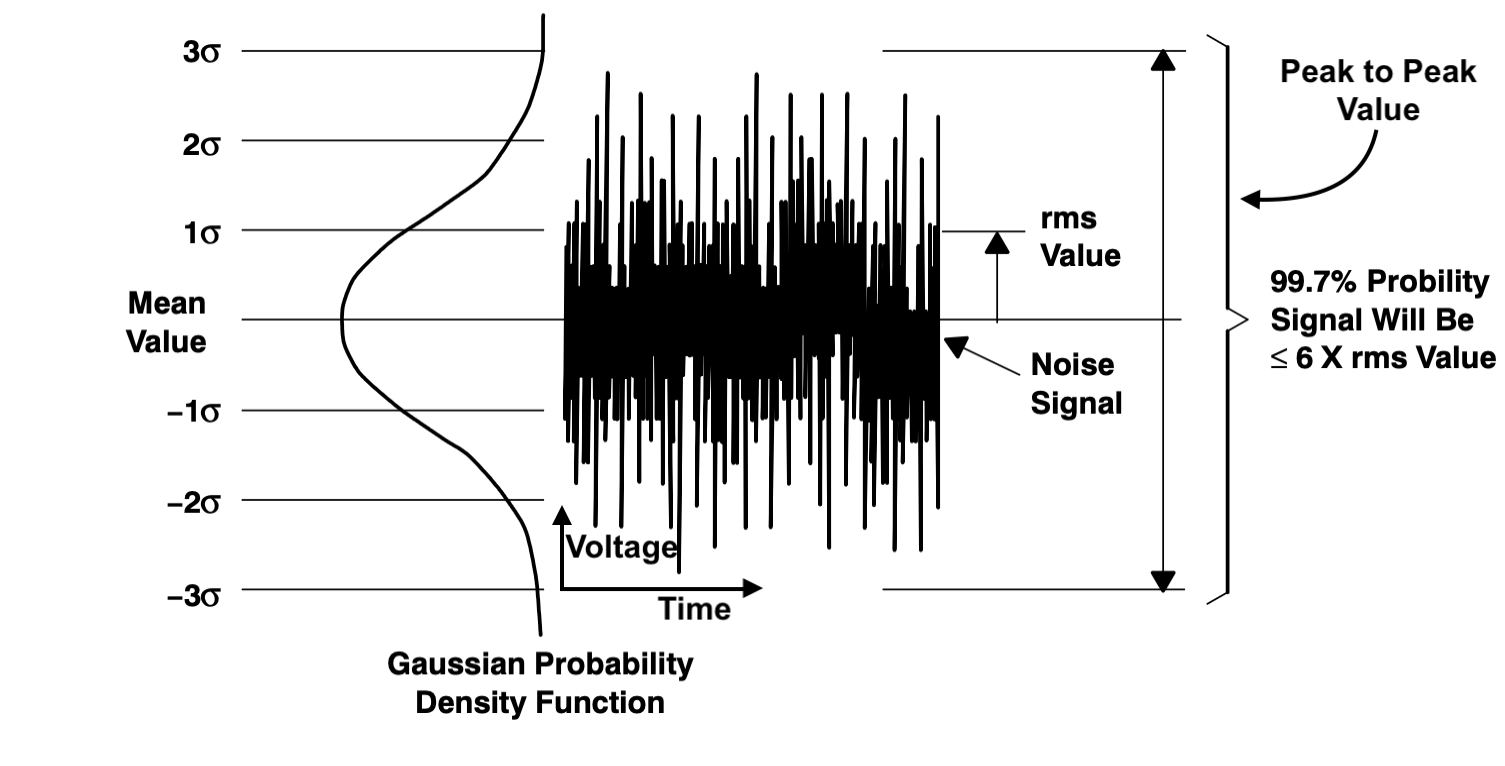
Peak-to-peak noise (Vpp) is the difference between the maximum positive and maximum negative amplitude of a noise signal over a specific period. While RMS noise represents the average power or "effective" value of the noise, peak-to-peak noise indicates the total vertical "spread" you would see on an oscilloscope.
Given that the RMS value of a noise source is equivalent to its standard deviation (σ=Vrms), the peak-to-peak amplitude (Vpp) can be estimated statistically. To ensure the signal remains within these limits with probability, a crest factor of 6 is applied (Vpp = 6×Vrms), spanning from -3σ to +3σ. Depending on the required confidence level, this multiplier typically ranges from 3 to 6.
Frequency-Domain Noise Concepts
In electronics, noise is analyzed mostly in frequency domain. From frequency domain, it is possible to obtain the time domain Vrms or Vpp information.
Noise spectral density
The power spectral density (PSD) quantifies how much power a signal carries at a given frequency. The total average noise power Pn in a particular frequency band is found by integrating the PSD. In mathematics, voltage noise PSD is denoted by symbol Sv(f) and current noise PSD is denoted by symbol Si(f).
$$P_n=\int_{f_1}^{f_2}S_v(f)df$$
The relation between time domain Vrms (noise amplitude) and integrated noise power (Pn):
$$\cfrac{V_{rms}^2}{2R}=P_n$$
Average power of noise
$$P_x=\cfrac{1}{T}\int_{-T/2}^{T/2}x^2(t)dt=\int_{-\infty{}}^{+\infty{}}S_x(f)df$$
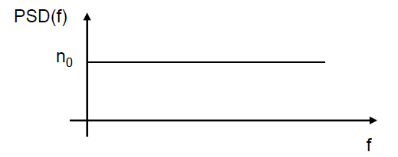
White noise
White noise is a random signal with equal power across all frequencies within a given bandwidth, characterized by a flat spectral density. Example of white noises are thermal noise of resistors, MOSFET channel noise, shot noise of p-n junctions etc.
Resistors have thermal noise which is frequency-independent (white) as shown below:
$$\text{PSD}(f)=4kTR$$
P-N junctions have shot noise which is also frequency-independent (white) as shown below:
$$\text{PSD}(f)=2qI_D$$
Colored noise or frequency-dependent noise
Colored noise is a random signal where power is not evenly distributed across frequencies, unlike white noise. It is generated by passing white noise through filters, resulting in frequency-dependent, correlated, and non-stationary signals. Key types include pink (1/f) noise and Brownian/red noise (1/f2).
Equivalent noise bandwidth
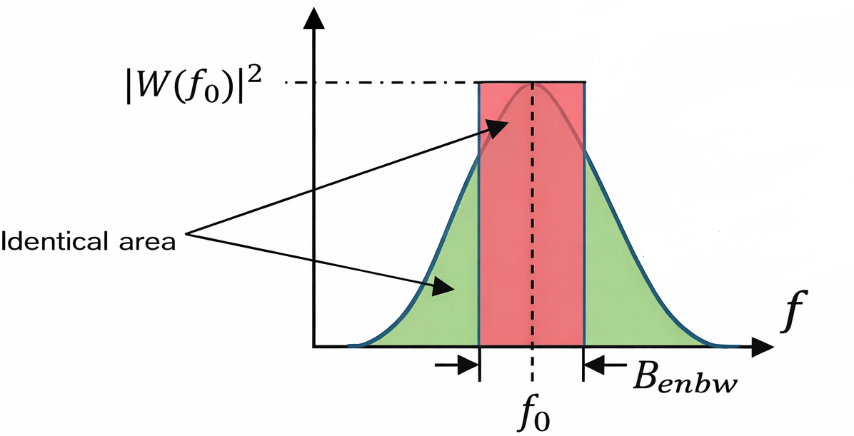
Equivalent noise bandwidth or noise bandwidth (BENBW or BN), is the width of an ideal rectangular filter that passes the same total noise power as a real filter. It is used to estimate total noise in circuits and systems, with values typically slightly higher than the 3-dB bandwidth. For example, the relationship between -3dB bandwidth and noise bandwidth for a single pole low pass filter is :
$$B_N=\cfrac{\pi}{2}\times{}f_{-3dB}\simeq{}1.57\times{}f_{-3dB}$$
Derivation
In case of bandpass filter, let's assume that f0 be the center frequency of the system. We assume that the filter has H(f0) uniform magnitude over the brick wall filter. In case of low-pass filter, H(0) is the DC output. $$\bar{v_n(t)^2}=|H(f_0)|^2B_n$$ $$\bar{v_n(t)^2}=\int_{0}^{\infty{}}|H(f)|^2df$$ $$\implies{}B_n=\cfrac{\int_{0}^{\infty{}}|H(f)|^2df}{|H(f_0)|^2}$$
Noise gain
From basic op-amp theory, two gains are defined: signal gain and noise gain. Signal gain depends on location of input and output port. For a noninverting amplifier, G = RF/RG + 1; for an inverting amplifier, G = -RF/RG. In both cases, the noise gain is identical and equals the noninverting gain expression: NG = RF/RG + 1. For noise gain, it is assumed that input referred noise voltage is located at non-inverting input of the amplifier.
Fundamental Noise Types
There are following fundamental noise types in electronic devices :
Thermal noise (Johnson–Nyquist noise)
Thermal noise, also known as Johnson–Nyquist noise, is the unavoidable electronic noise generated by the random thermal agitation of charge carriers (usually electrons) inside an electrical conductor at equilibrium, occurring even without any applied voltage. It is proportional to temperature (T), resistance (R), and bandwidth (ΔB). The phenomenon was first measured by John B. Johnson at Bell Labs in 1928 and explained theoretically by Harry Nyquist. Like shot noise, thermal noise is spectrally flat or has a uniform power density, but thermal noise is independent of current flow.
Found in resistors and MOSFETs, and is a major limiting factor in sensitive electronic equipment. Thermal noise has a uniform or “white” PSD.
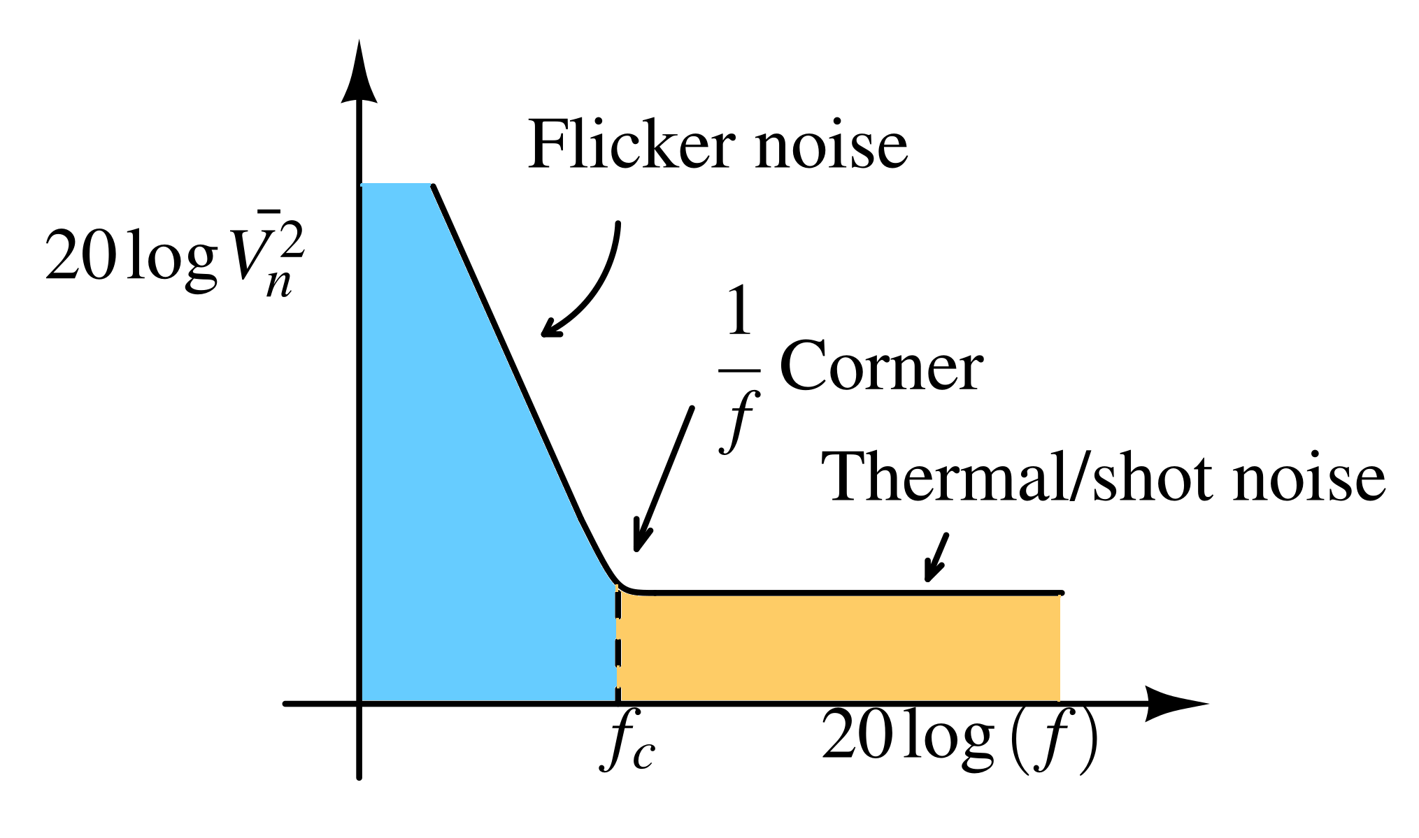
Flicker noise (1/f noise)
Flicker noise arises from surface imperfections and dangling bonds (acting as carrier scattering centers) at the interface between the gate oxide and silicon substrate in MOSFETs. Random trapping and release of charge carriers in these defects introduces current fluctuations. Flicker noise (1/f noise) magnitude increases as frequency decreases. It can be reduced by enlarging transistor dimensions, though this increases area and parasitic capacitances, creating a design trade-off.
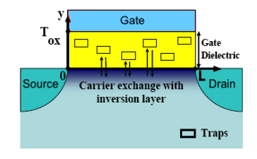
PMOS devices typically exhibit lower flicker noise than NMOS due to a smaller process-dependent constant, which is why PMOS transistors are often preferred at the input stage.
Similar to thermal noise, flicker noise can be modeled using equivalent voltage source at the gate of MOSFET :
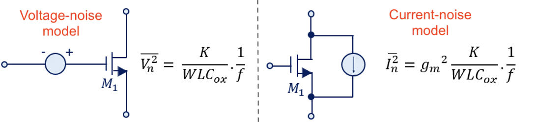
$$\cfrac{\bar{V_n}^2}{\Delta{}f}=\cfrac{K_F}{C_{ox}WL}\cfrac{1}{f}$$
Devices with lower flicker noise
Devices in which conduction occurs primarily through the bulk rather than the surface typically exhibit lower flicker noise (BJTs, JFETs etc).
Hooge model
F N Hooge10 proposed that 1/f noise is essentially a bulk phenomenon not a surface effect alone. He also proposed formula similar to 1/f for resistance fluctuations: $$R_n^2=\cfrac{\alpha{}_H}{N}\cfrac{R^2}{f}$$
Chopper amplifier
Flicker noise can really hamper measurement of tiny signals (< μV range). Chopper amplifiers have almost zero flicker noise due to chopping technique. Some examples of chopper amplifiers are OPA4833, ADA4523.
Shot noise
Shot noise is always associated with current flow. It was proposed by Schottky to measure the electron charge in 1918. Shot noise results whenever charges cross a potential barrier, like a pn junction. Thus the instantaneous current, i, is composed of a large number of random, independent current pulses with an average value, iD. Shot noise is generally specified in terms of its mean-square variation about the average value. The power spectral density of shot noise is :
$$\text{PSD}=\cfrac{i_n^2}{\Delta{}f}=2qI_D$$
Shot noise is spectrally flat or has a uniform power density, meaning that when plotted versus frequency, it has a constant value. Shot noise is independent of temperature. The PSD has units of A2/Hz.
It is the dominant noise source in Diodes (including LEDs, photodetectors4 etc) and BJTs 2.
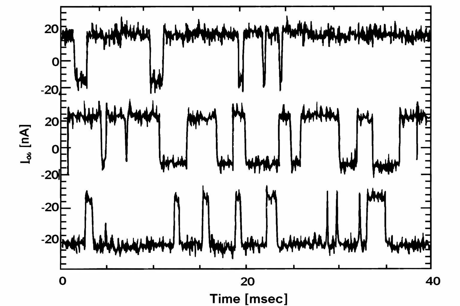
Burst noise (popcorn noise)
Burst noise, also called popcorn noise, appears to be related to imperfections in semiconductor material and heavy ion implants. It is caused by discrete modulation of the channel current caused by the capture and emission of a channel carrier. Burst noise makes a popping sound ("like pops while making popcorn") at rates below 100 Hz when played through a speaker. It is frequently found in BJTs.
Avalanche Noise
Avalanche noise (IAVL) arises when a p–n junction operates in reverse breakdown. The strong electric field in the depletion region accelerates carriers to high kinetic energies. Upon colliding with lattice atoms, they generate additional electron–hole pairs through impact ionization. These random multiplication events produce large, stochastic current pulses, similar to shot noise but significantly more intense. The avalanche noise can be modelled as :
$$\cfrac{\bar{i_{n}}^2}{\Delta{}f}=2qI_{R}M^2F$$
Where,
IR is the reverse biased current flowing through p-n junction. M is the gain (M=1 for non-multiplying diode)7.
Device-Specific Noise
Most commonly used device noise model are mentioned below :
Resistor noise
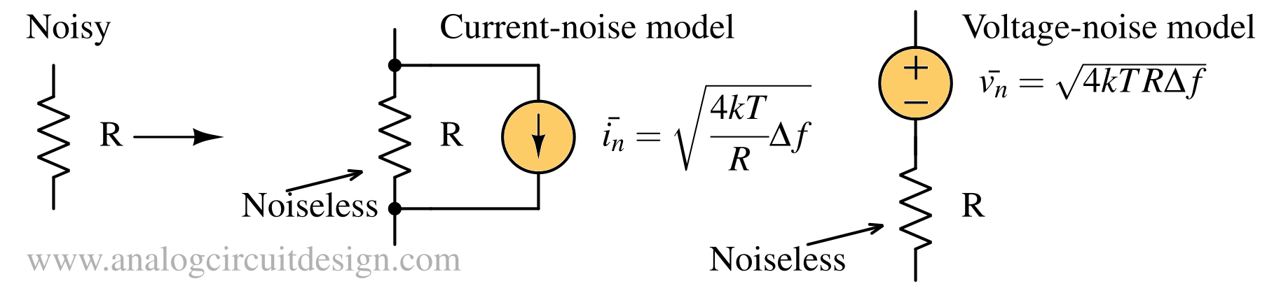
The power spectral density (PSD) of thermal noise in resistors is :
$$\text{PSD}=\cfrac{v_n^2}{\Delta{}B}=4kTR$$
The voltage PSD has units of V2/Hz.
The RMS voltage is given by (derived from above equation) :
$$v_n=\sqrt{4kTR\Delta{}B}$$
A fifty ohm resistor adds about 1 nV/√Hz of thermal noise density.
Diode noise
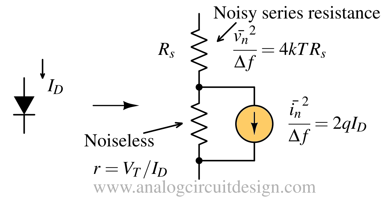
A diode has following noise in decreasing order of severity:
- Shot noise of p-n junction
- Thermal noise of contact series resistance
- Flicker noise at low frequencies
Shot noise is the dominant noise source in a forward-biased diode. A 1mA current through a p-n junction has about 18pA/√Hz of shot noise density.
MOSFET noise
A MOSFET has following noise sources in decreasing order of severity:
- Channel noise (thermal noise)
- Flicker noise
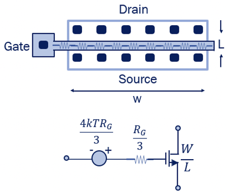
- Gate resistance noise
The major noise contributor in MOSFET is the channel noise. It is modelled as shown below:
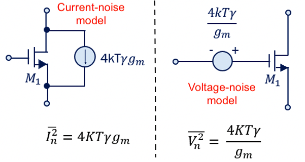
The noise is directly proportional to temperature. The PSD (if modelled as current noise) is :
$$\cfrac{\bar{i_n^2}}{\Delta{}f}=4kT\gamma{}g_m$$
γ is the excess noise coefficient. γ is 2/3 for long channel transistors (L>1μm). γ rises to 3 for short channel transistors.
The major noise contributor at low frequency is the flicker noise. It is modelled as:
Another noise contributor in MOSFET is the gate resistance. It is modelled as a resistor noise:
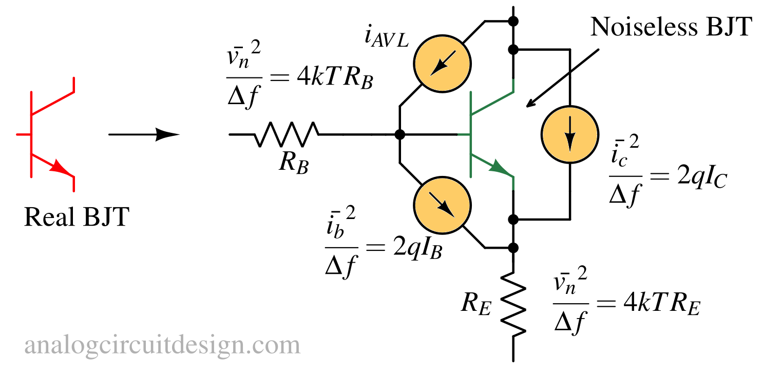
BJT noise
A BJT has following noise in decreasing order of severity:
- Collector-emitter shot noise
- Collector-emitter flicker noise
- Base bulk resistance thermal noise
- Base-emitter shot noise
- Collector-base avalanche noise
- Emitter contact resistance thermal noise
JFET noise
A JFET has following noise in decreasing order of severity:
- Channel thermal noise (4kTγgm)
- Channel flicker noise (KDID/f)
- Gate shot noise
- Gate drain avalanche noise (iAVL)
JFET has a junction at the gate therefore it has a shot noise component there. The CGS parasitic capacitor becomes dominant current noise at higher frequency. The capacitor is noiseless however the current sources which sets the DC current of JFET has noise. These noises couples to the gate through the CGS capacitor. The channel noise is similar to a MOSFET.
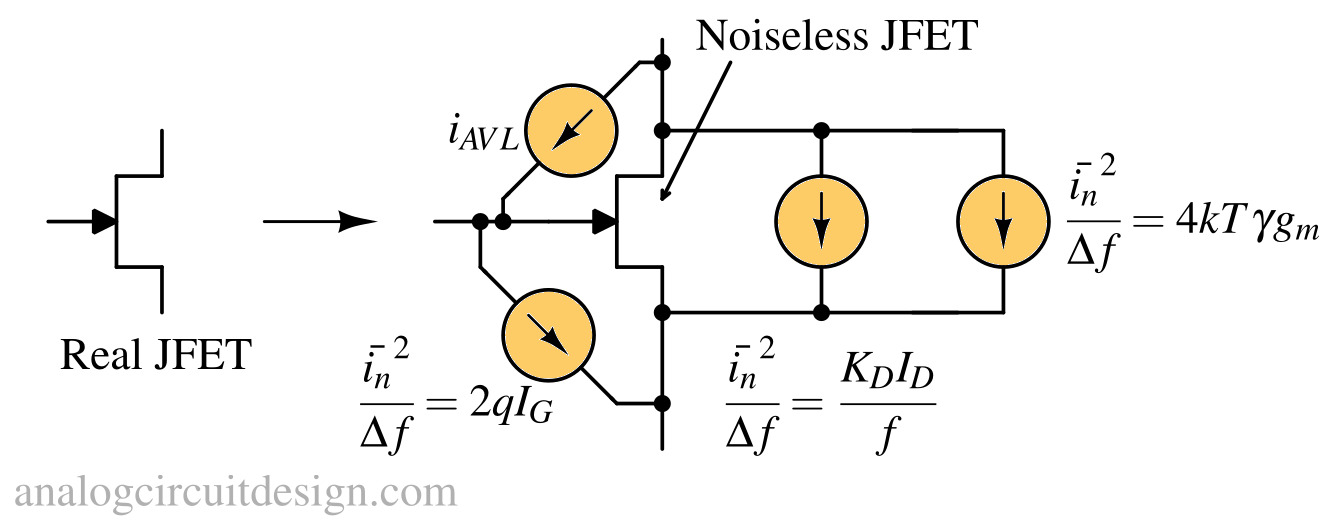
The flicker noise component is usually 4-5X lower than MOSFET because the carrier flow through bulk instead of surface. However, the flicker noise is higher than BJT.
Addition of different noise sources
With multiple noise sources in a circuit, the signals must be combined properly to obtain the overall noise signal. Consider the example of two resistors, R1 and R2, connected in series. Each resistor has a noise generator associated with it as shown in below figure where:
$$\bar{V_1^2}=\int{}4kTR_1df$$
and,
$$\bar{V_2^2}=\int{}4kTR_2df$$
Filtered noise
Noise output spectral density is a function only of the magnitude of the transfer function, and not its phase.
Noise of an RC Circuit
As shown earlier, the resistor has a white band noise. If a capacitor is added, like in a low-pass filter, the noise attenuates for higher frequency. Capacitor itself does not add noise, however it shapes the PSD. The noise amplitude can be found by integrating the PSD across frequency. The PSD is shaped due to low pass filter.
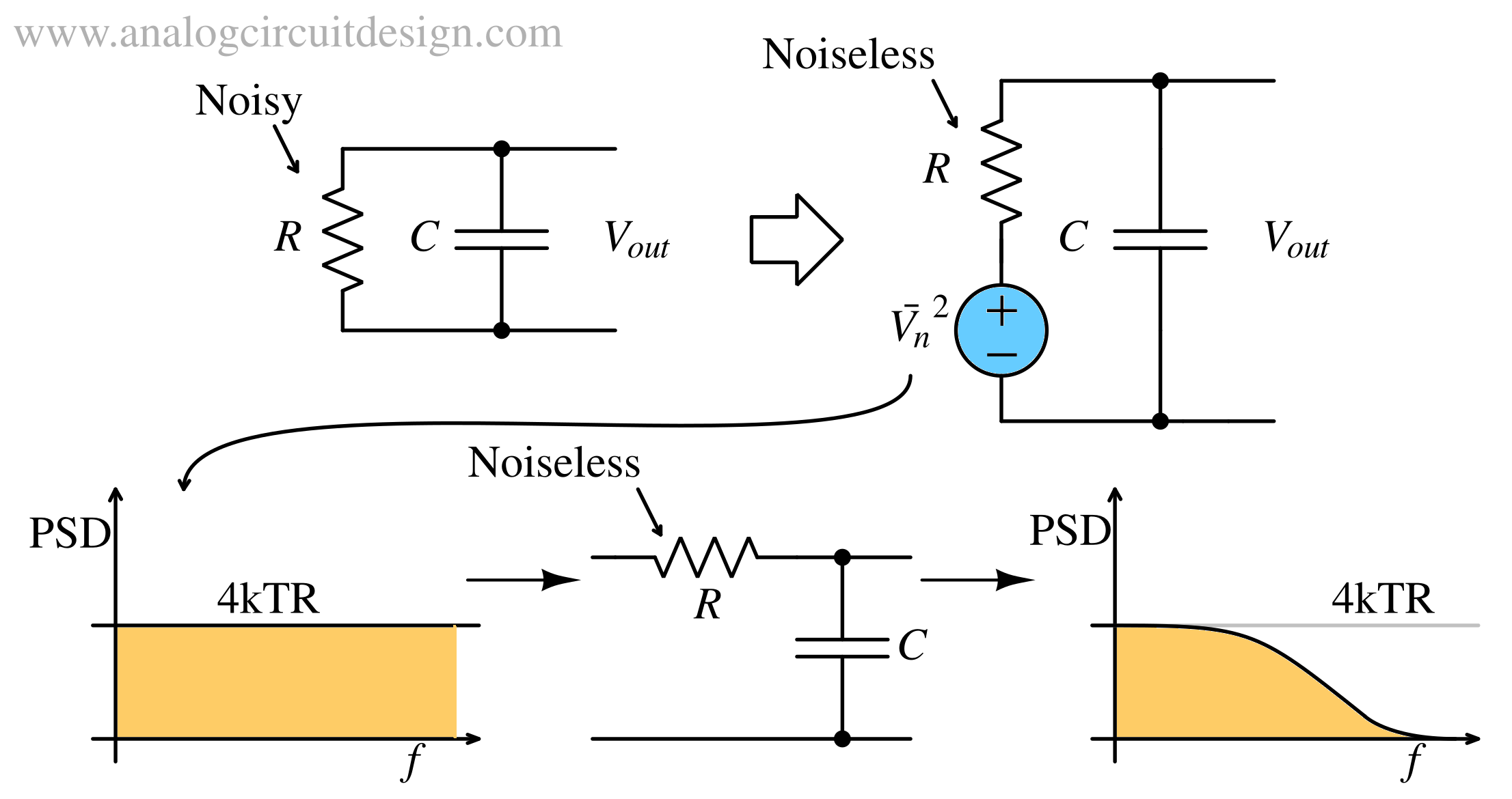
Transfer function of RC low pass filter:
$$A(s)=\cfrac{V_{out}(s)}{V_{in}(s)}=\cfrac{1}{1+sRC}$$
$$V_{out}^2(f)=|A(j2\pi{}f)|^2V_{in}(f)=\cfrac{1}{1+4\pi{}^2f^2R^2C^2}4kTR$$
To calculate total noise power, integration is required over frequencies.
$$V_{out,rms}^2=\int_0^{\infty}\cfrac{4kTR}{1+4\pi{}^2f^2R^2C^2}$$
Using,
$$\int{}\cfrac{dx}{x^2+1}=\tan{}^{-1}x$$
$$V_{out,rms}^2=\cfrac{2kT}{\pi{}C}\tan^{-1}(2\pi{}fRC)\Big|_{f=0}^{f=\infty{}}=\cfrac{kT}{C}$$
The total integrated noise is independent of resistor. It is only dependent of capacitor, even though it is generated by the resistor.
Intuition
When R increases, thermal noise increases too but the cut-off frequency decreases, leading to a constant area, solely dependent on capacitor.
Filter noise, often referred to as (kT/C) noise, is not a fundamental noise source but rather the result of thermal noise in the presence of a filtering capacitor. The filtering network may consist of a discrete RC combination or intrinsic device elements such as the channel resistance and drain capacitance of a MOSFET. Including both thermal noise and (kT/C) noise in the same analysis would lead to double counting.
Noise Modeling & Analysis
Small-signal noise model
Noise is treated as small-signal. Every device is linearized at its operating point to calculate the noise.
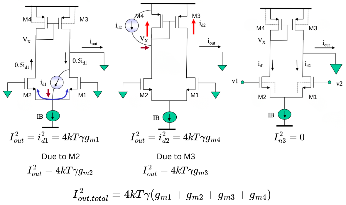
Output-referred noise
Output-referred noise is the total RMS noise PSD measured at an amplifier's output, resulting from all internal noise sources. Using superposition, the noise contribution of each transistor is analyzed individually while the others are deactivated. Standard circuit analysis techniques can be applied, but noise must ultimately be evaluated in terms of power. Since each noise source represents the RMS value of an uncorrelated random signal, the total noise is obtained by summing the individual noise powers.
Input-referred noise
Input-referred noise is a modeling technique that represents all noise sources of a circuit as equivalent voltage and current noise sources at the input. This way, the minimum detectable signal at the input becomes the input-referred noise. To find the input referred noise, first output referred noise needs to be calculated first.
If the gain block is a voltage controlled current source, the input should be a voltage and output is a current. The gain of the transconductor is gm1. The input referred noise would be :
$$v_{n}^2=\cfrac{I_{out,total}^2}{g_{m1}^2}$$
Correlated and Uncorrelated noise
Correlated noises have same origin in a circuit. They may have different amplitudes but have in-phase or out-of-phase relationship. They add directly to amplitude. Uncorrelated noise is independent, random, and adds on a power basis not amplitude basis.
With multiple uncorrelated noise sources, combined output is also uncorrelated.
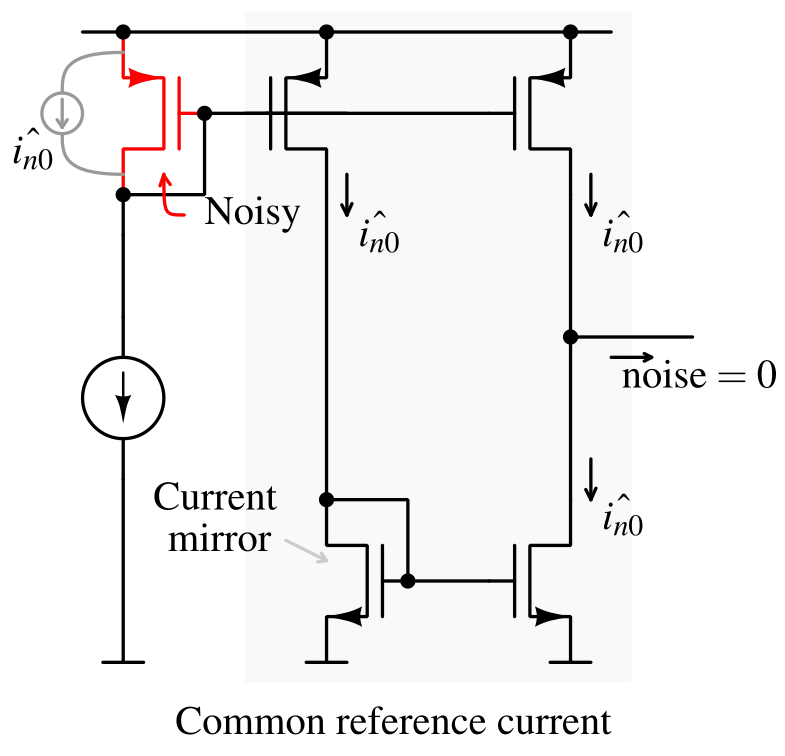
Common mode noise
Noise that appears with the same amplitude and phase on both lines of a differential signal is referred to as common-mode noise.
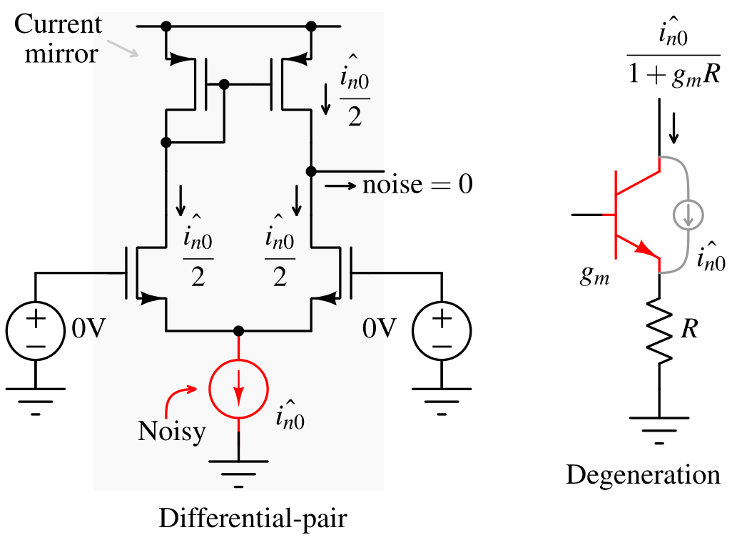
A very common example is the input differential pair of opamp (shown above). The tail current source is common mode noise which appear equally at both the input transistors. The noise from left transistor is mirrored by the top mirror which cancels the noise current through right transistor. Hence, total output current is zero.
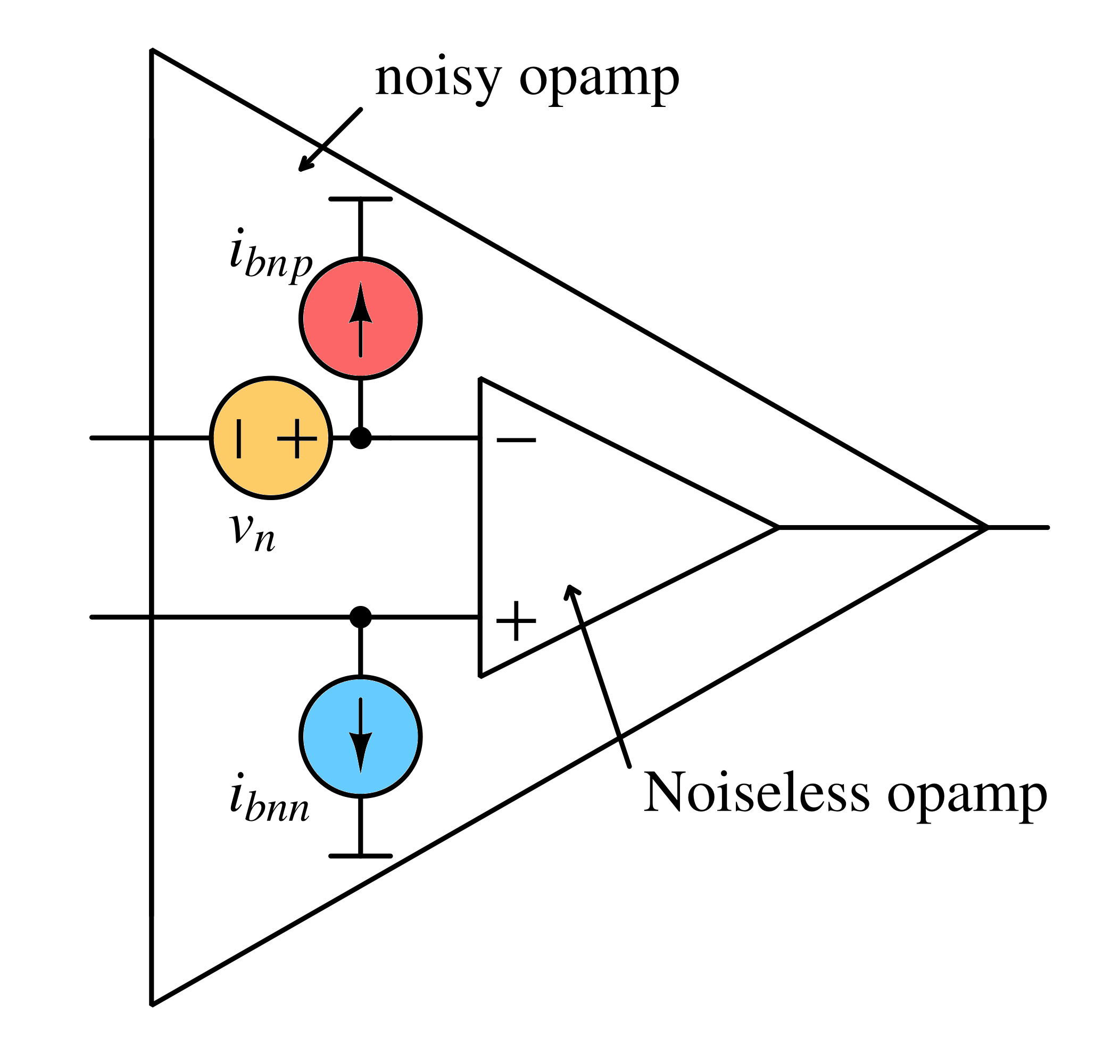
Noise in an Operational amplifier
Noise of operational amplifier depends majorly on the input stage because of its very high gain. Within the input stage, the input transistors are critical. Input transistors could be JFET, CMOS, BJT etc.
Noise measurement
Noise measurement is done using a spectrum analyzer which plots the PSD with frequency.
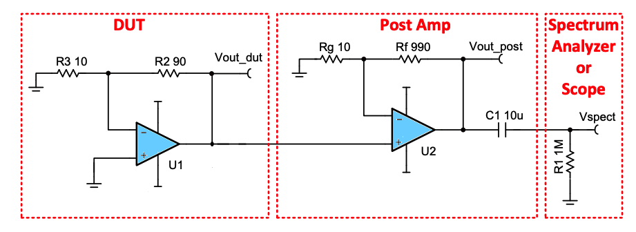
In some situations, an oscilloscope or spectrum analyzer may lack the sensitivity to measure very small noise levels. A noise measurement post-amplifier is therefore used to amplify the output noise of the device under test (DUT), enabling accurate measurement with standard test equipment. Such a circuit must have a very low noise floor and sufficient bandwidth to properly characterize the DUT. Select a post-amplifier that has an output noise at least 3x lower than the DUT noise floor to minimize noise.
Interference noise
Interference is deterministic and theoretically predictable, though it remains difficult to model in practice. Examples :
- Power supply noise
- Electromagnetic interference (EMI)
- Substrate coupling
Some solutions to these noises are :
- Fully differential circuits
- Layout techniques
-
https://people.engr.tamu.edu/spalermo/ecen474/lecture12_ee474_noise.pdf ↩
-
https://123.physics.ucdavis.edu/shot_files/ShotNoise.pdf ↩
-
https://web.mit.edu/8.13/www/JLExperiments/JLExp43.pdf ↩
-
https://www.rp-photonics.com/shot_noise.html ↩
-
K. K. Hung, P. K. Ko, C. Hu and Y. C. Cheng, "A physics-based MOSFET noise model for circuit simulators," in IEEE Transactions on Electron Devices, vol. 37, no. 5, pp. 1323-1333, May 1990, doi: 10.1109/16.108195. ↩
-
https://leachlegacy.ece.gatech.edu/ece6416/Labs/exp05.pdf ↩
-
https://upload.wikimedia.org/wikipedia/commons/9/98/Noise_characteristics_of_an_avalanche_photodiode_%28IA_noisecharacteris00kime%29.pdf ↩
-
A. Balandin, K. L. Wang, A. Svizhenko and S. Bandyopadhyay, "The fundamental 1/f noise and the Hooge parameter in semiconductor quantum wires," in IEEE Transactions on Electron Devices, vol. 46, no. 6, pp. 1240-1244, June 1999, doi: 10.1109/16.766892. ↩
-
Jimmin Chang, A. A. Abidi and C. R. Viswanathan, "Flicker noise in CMOS transistors from subthreshold to strong inversion at various temperatures," in IEEE Transactions on Electron Devices, vol. 41, no. 11, pp. 1965-1971, Nov. 1994, doi: 10.1109/16.333812. ↩
-
https://web.mit.edu/klund/www/papers/UNP_noise.pdf ↩
-
J. B. Johnson. The schottky effect in low frequency circuits. Physical Review, 26(1):71–85, July 1925 ↩