Operational amplifier (Opamp) Architectures
Understanding the internal architecture of opamp helps understanding the datasheet and enable us to select the optimal opamp for our application.
Two stage opamp
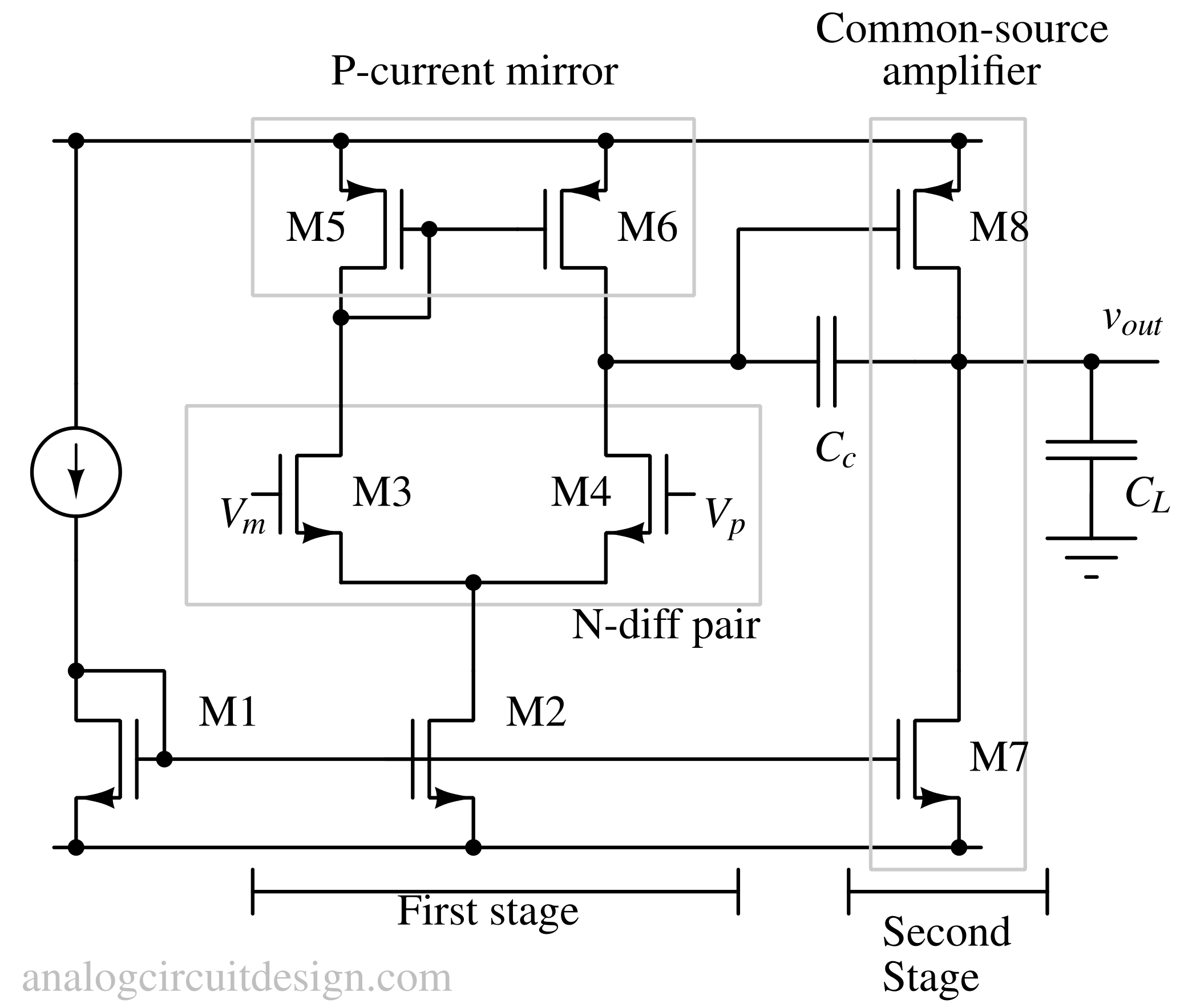
The first stage is typically a differential amplifier, which offers high input impedance, good common-mode rejection, and initial voltage gain. The second stage is a gain or output stage, usually a common-source or common-emitter amplifier, designed to further increase gain and drive the load. Frequency compensation, often implemented using Miller compensation, is essential to ensure stability.
Three stage opamp

Three stage opamps are designed to achieve very high voltage gain and improved output drive capability compared to two-stage designs. The first stage is usually a differential input stage that provides high input impedance and good common-mode rejection (CMRR). The second stage adds substantial voltage gain. It is added to isolate the output stage affecting the input stage. The third stage acts as an output buffer (non rail to rail output) or a transconductor (rail to rail output stage), improving load-driving ability and output swing. Because additional stages introduce more poles, frequency compensation techniques such as nested Miller compensation are required to ensure stability.
Feedforward opamp
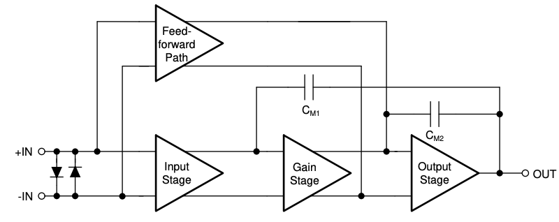
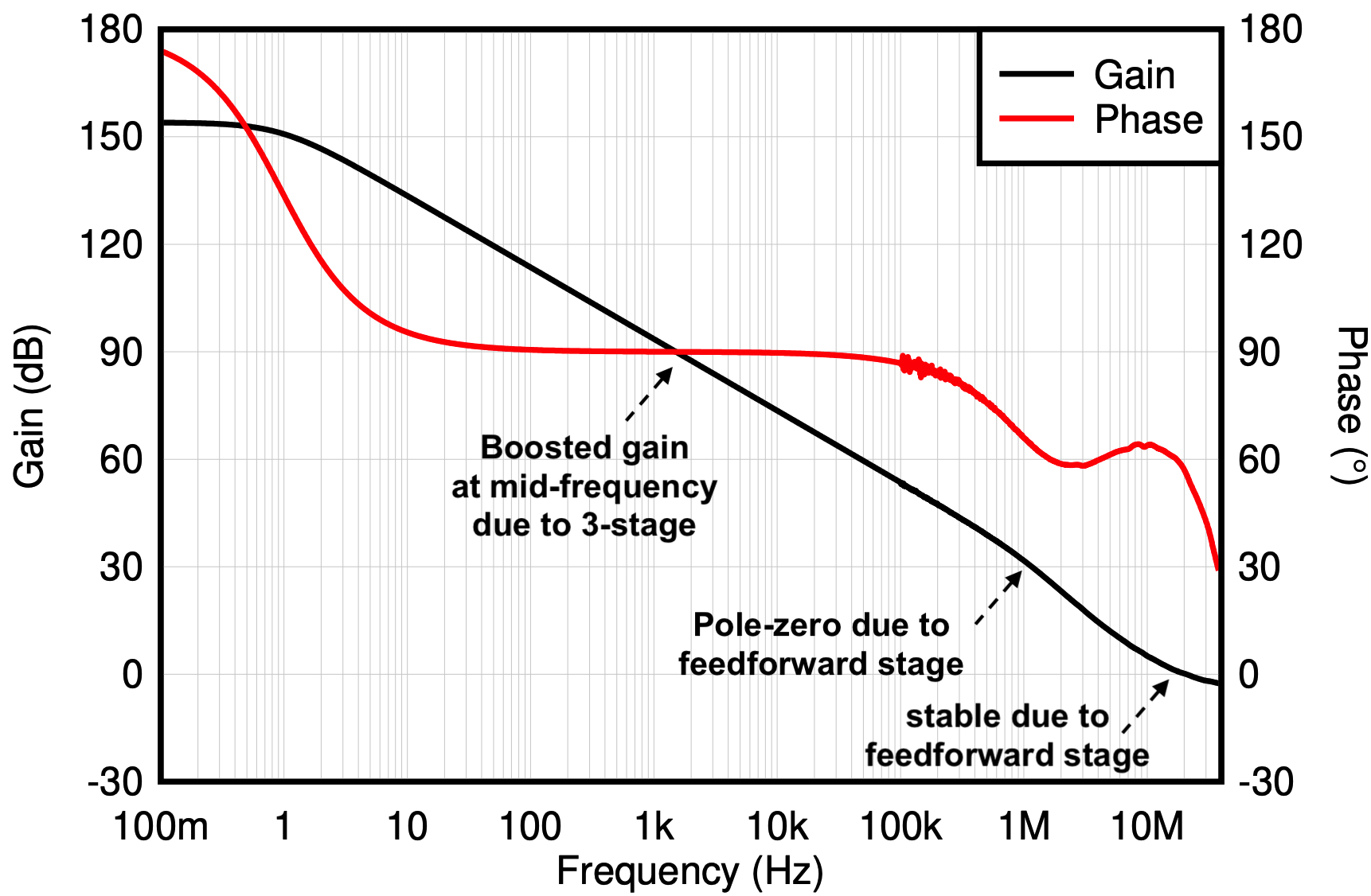
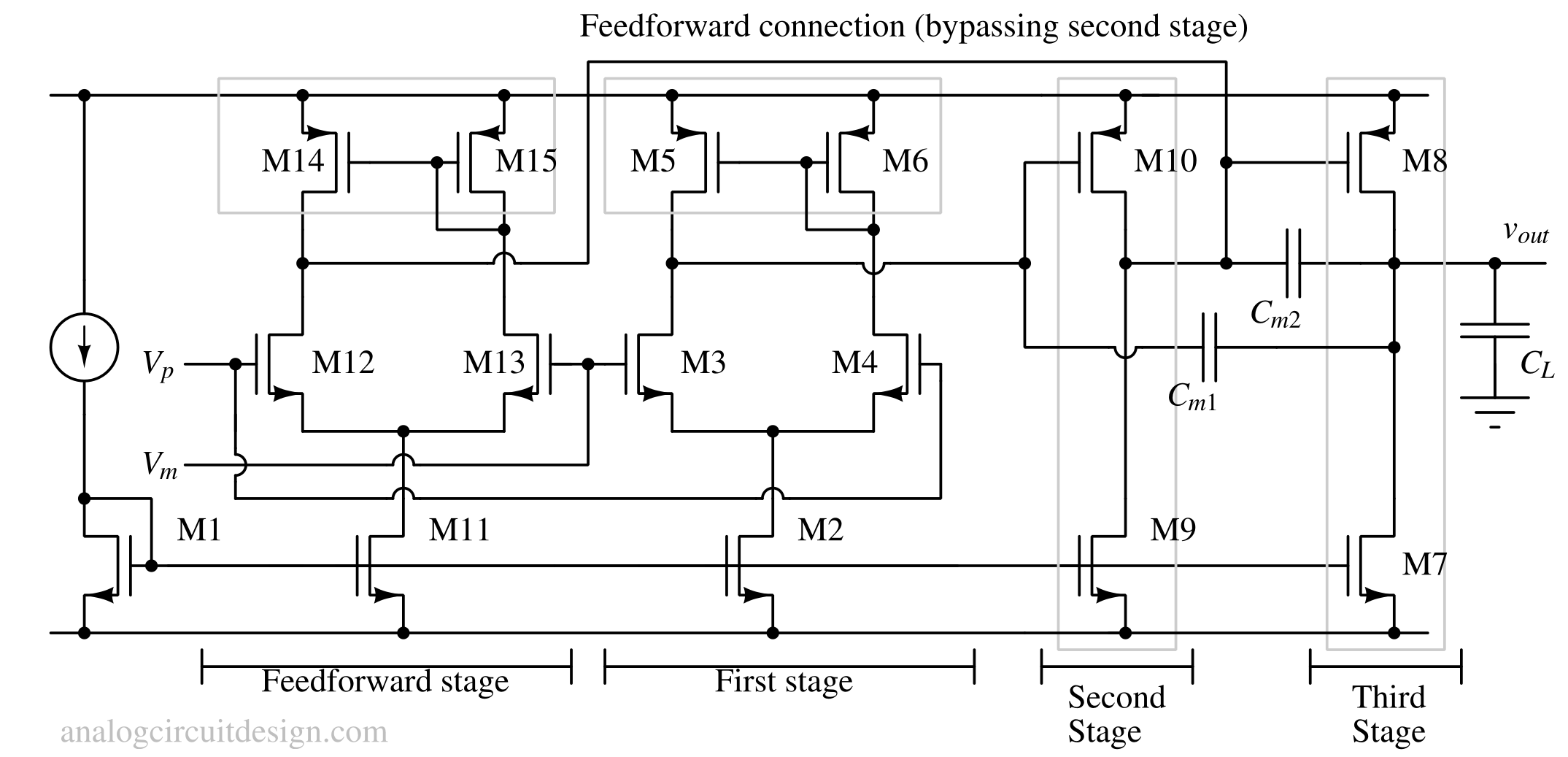
A feedforward op-amp architecture uses an additional signal path that bypasses two gain stages (as shown above) in a 3-stage opamp to improve stability (phase margin and gain margin). Unlike conventional designs that rely only on feedback, feedforward paths allow fast signal components to reach the output directly, reducing phase delay and improving slew rate. This technique enhances bandwidth, transient response, and stability without significantly increasing power consumption. Feedforward op-amps are especially useful in high-speed and wideband applications, such as audio amplifiers. By minimizing internal signal delay, feedforward architectures achieve better linearity and faster settling compared to traditional multi-stage op-amps.
Opamps like OPA1656 are feedforward stage amplifiers.
A transistor level implementation of feedforward opamp is shown below.
Input stage
Non Rail-to-Rail Input stage
A lot of operational amplifiers cannot support input signal swing till supply voltage rails. These are called non rail to rail opamps.
This limitation arises from the input differential pair and tail current source topology, where the tail current source requires a minimum voltage headroom to operate correctly. As the input approaches either supply rail, the tail current source turn off, leading to distortion or loss of amplification (increase in Vos). Non rail-to-rail input op-amps are commonly used if the input swing is known. These op-amps provides better noise and precision for a given power budget. Works for inverting amplifier.
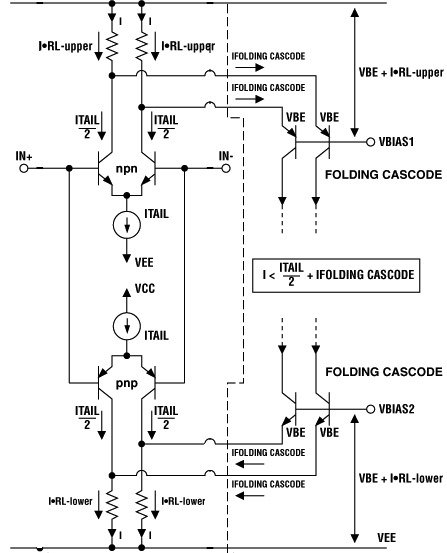
Negative rail input stage
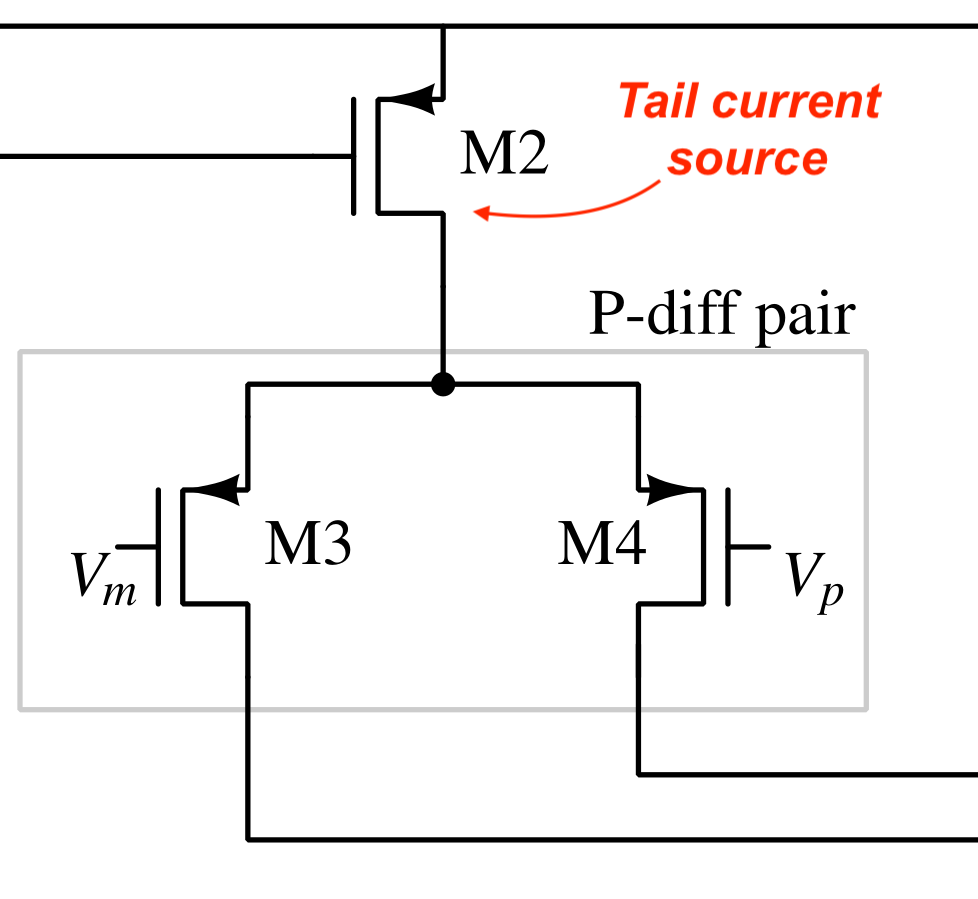
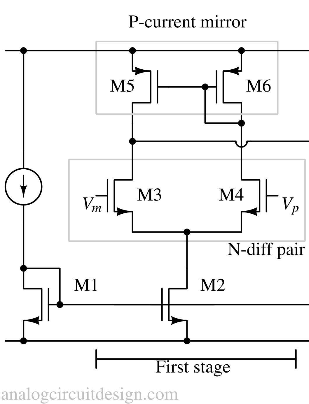
This kind of input stage allows the input voltage to swing down to, or very close to, the negative supply rail. This capability is important in single-supply systems where signals are referenced to ground, which often serves as the negative rail. Such input stages are typically implemented using PNP bipolar transistors or PMOS differential pairs (shown above as M3 and M4), which remain active at low input voltages. While the input can approach the negative rail, it usually cannot reach the positive rail due to tail current source (as shown above using PMOS transistor M2), making the op-amp non rail-to-rail. Negative rail input op-amps are widely used in low-side current sensing applications.
Positive rail input stage
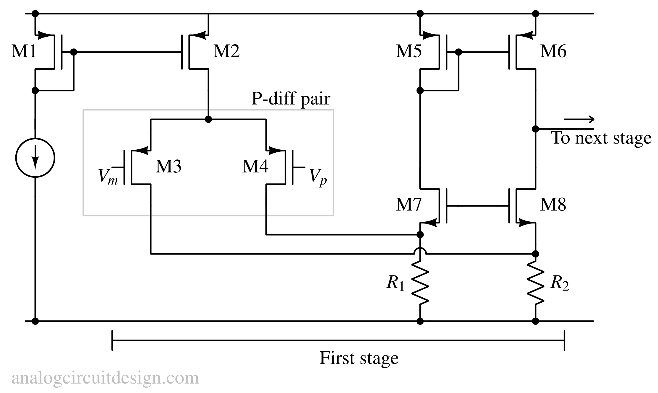
A positive rail input stage in an operational amplifier allows the input voltage to swing up to, or very close to, the positive supply rail. This feature is useful in single-supply circuits where signals operate near the upper supply voltage. Such input stages are commonly implemented using NPN bipolar transistors or NMOS differential pairs (shown above as M3 and M4), which function well at higher input voltages. While the input can approach the positive rail, it cannot typically reach the negative rail because of bottom tail current source (as shown above using NMOS transistor M2). This makes the op-amp non rail-to-rail. Positive rail input op-amps are often used in high-side sensing, level detection, and comparator-like applications where upper-rail signal handling is required.
Intermediate rail input stage
Rail-to-Rail Input stage
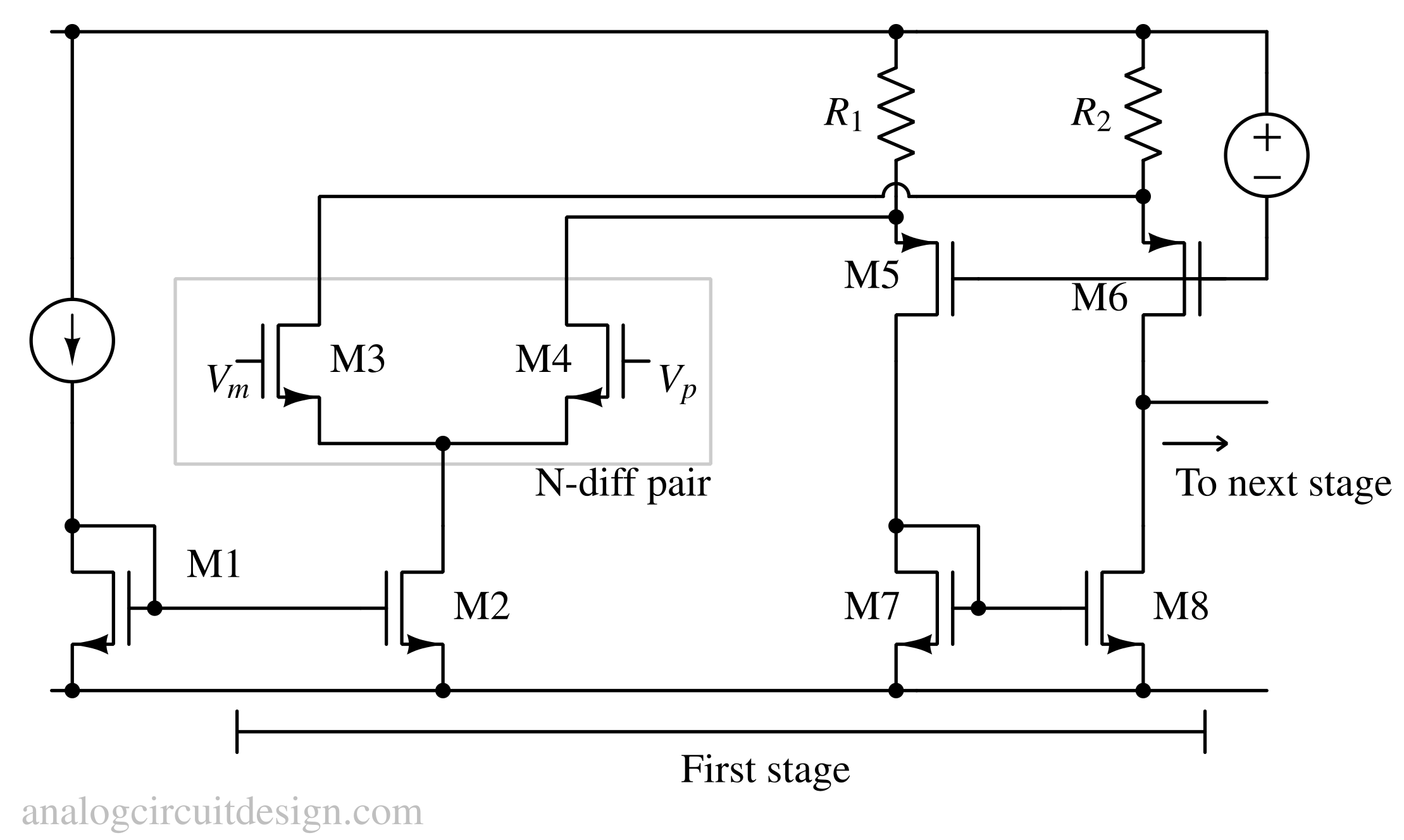
A rail-to-rail input stage allows an operational amplifier to accept input voltages that span nearly the entire supply voltage range, from the negative rail to the positive rail. This is especially important in low-voltage, single-supply systems where signals are closer to supply voltages (either VCC or VEE). Rail-to-rail input stages are commonly implemented using complementary differential pairs (Negative rail input stage + Positive rail input stage) that operate over different portions of the input range. As the input approaches either supply rail, one pair gradually takes over from the other, ensuring continuous operation.
These are needed for non-inverting amplifier configuration, where the input stage sees the full signal swing.
Intermediate stage
Gain stage
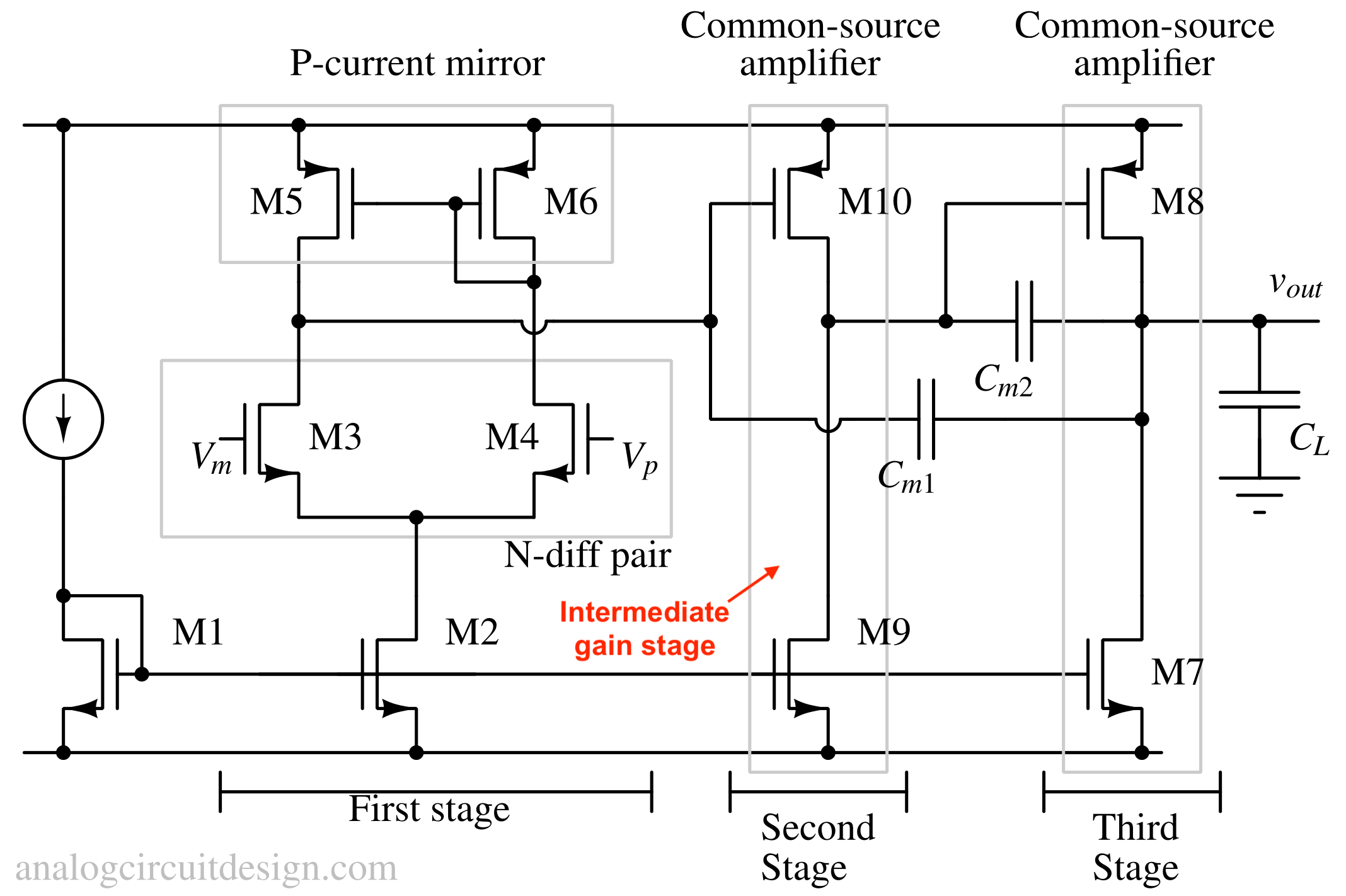
Sometimes open loop gain is not enough using two-stage amplifier. Higher open-loop gain has several benefits like systematic offset does not change much with output load and temperature. Therefore an intermediate gain stage (e.g., common-emitter amplifier, common-source amplifier) is inserted between a two-stage amplifier. This converts a two-stage amplifier into a three-stage amplifier as shown below.
Common mode feedback stage
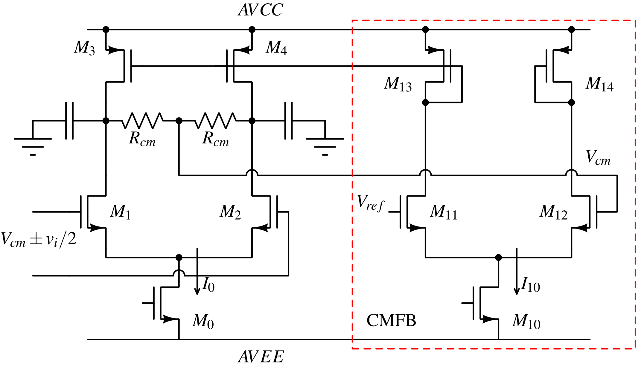
Any fully differential stage needs a common mode feedback circuit. A fully differential stage means, input is differential and output is differential as well. If first stage is fully differential, then first stage needs a common mode feedback circuit.
Why we need common mode feedback circuit ?
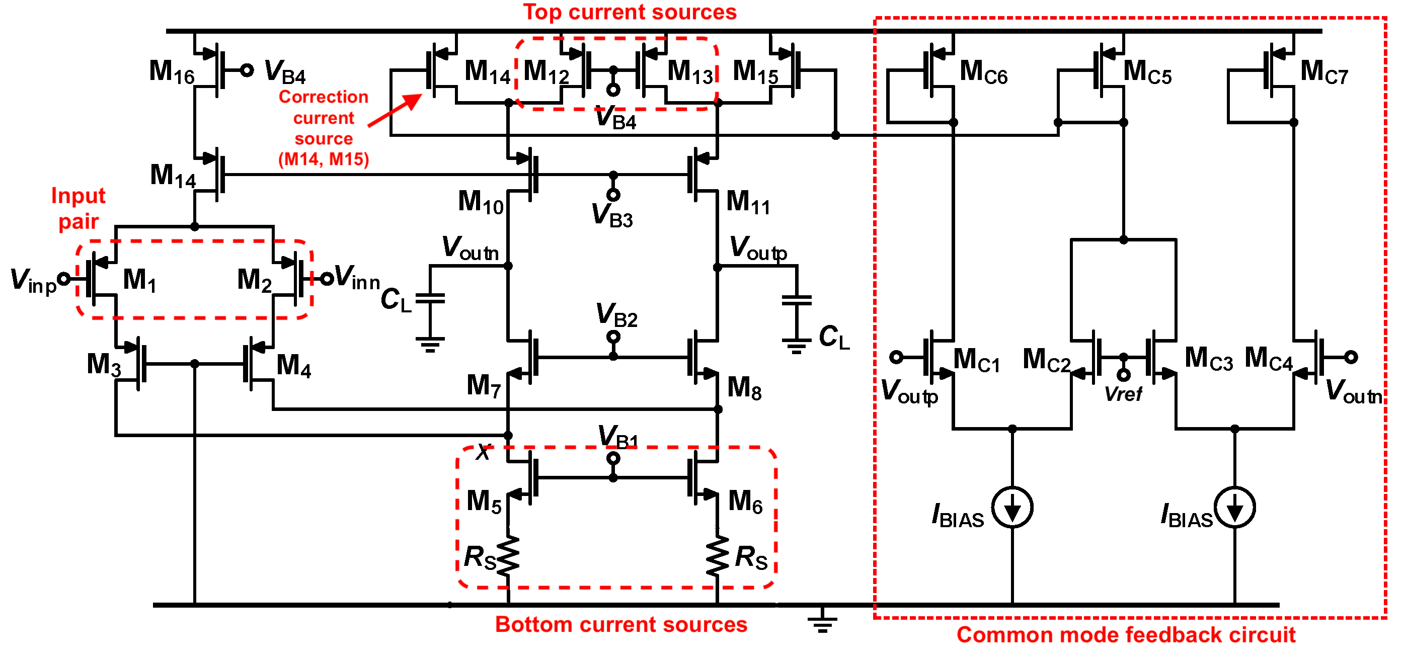
Usually the outputs of fully differential amplifiers/stage are current sources. There is a top current source which source current to the next stage, and bottom current source which sinks current. If there is a mismatch between top and bottom current source, e.g., top current source is higher than the bottom current source, the output continously rises till it saturates. There is no mechanism to stop the output rising. Even with outermost feedback loop, we cannot stop because input stage is fully differential and not sensitive to common mode shifts. A common mode feedback (CMFB) circuit senses this output rising and it adds necessary extra current in the circuit to equalize top and bottom current source. A CMFB holds the value to a reference called VCM.
Output stages
There are two kind of output stages. Rail-to-Rail output stage and non Rail-to-Rail output stage :
Rail-to-Rail output stage
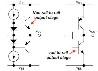
A rail-to-rail output stage in an operational amplifier allows the output voltage to swing very close to both the positive and negative supply rails. This capability is essential in low-voltage and single-supply systems, where maximizing output signal range is critical. Rail-to-rail output stages are typically implemented using complementary (PNP and NPN together) push–pull transistor pairs. Common-emitter (M1 and M2) or common-source stages are used to make these push-pull (class-AB) stages. While they greatly improve output swing, the output may still fall a few millivolts short of the rails depending on load current and transistor type (see claw-curve).
These opamps consume higher power than non rail-to-rail output stage for similar bandwidth. If your application does not need signal to go near rail, consider non rail-to-rail opamps.
Non Rail-to-Rail output stage
A non rail-to-rail output stage cannot drive its output voltage all the way to the supply rails and requires some headroom (typically 1V to 2V) at both the positive and negative ends. This limitation is due to the output transistor topology, such as emitter followers (common collector) or source followers, which need voltage across the devices to remain in active operation. It provides higher speed for lower power power than the rail to rail output stage.
Compensation schemes
To ensure transient stability (controlled overshoot and ringing) and avoid oscillations, operational amplifiers have to be frequency compensated using compensation capacitors (Cc). Some common compensation schemes are listed below:
Dominant pole compensation

Dominant pole compensation is a fundamental compensation technique used in operational amplifiers. It works by intentionally introducing a low-frequency pole that dominates the amplifier’s frequency response, causing the gain to hit 0dB gain at 20 dB/dec (before non-dominant poles arrive). This separation improves phase margin and prevents oscillations. Dominant pole compensation is commonly implemented using internal or Miller compensation capacitors in op-amp designs. If succeding stage is a high gain transcondutance stage, the dominant pole compensation alone in not very efficient. It does not split-poles like Miller compensation. To achieve pole-splitting, Miller compensation is more popular where succeding stage is high gain transconductor stage.
Miller compensation

Miller compensation is a widely used frequency compensation technique in operational amplifiers to ensure closed-loop stability. It involves placing a capacitor between the output and input of a high-gain stage, typically between the output of first stage (which is input of second stage) and output of second stages of a two-stage op-amp. This capacitor creates a dominant low-frequency pole and introduces pole-splitting, pushing higher-frequency poles away to improve phase margin. However, it can limit bandwidth and slew rate due to the large effective capacitance seen at the input, requiring careful trade-offs in high-speed op-amp designs.
Decompensated opamps

Decompensated opamps are not internally frequency compensated for unity-gain stability. Unlike unity-gain–stable op-amps, decompensated op-amps are designed to be stable only above a specified minimum closed-loop gain (for example, gain ≥ 5 or ≥ 10). By reducing internal compensation capacitance, these amplifiers achieve higher bandwidth for higher gain (in comparison to unity-gain stable amplifiers), faster slew rate, etc. However, using them at low gains can lead to oscillations or instability.
If the application requires a closed-loop gain of 10 or higher, a decompensated amplifier that is stable at a gain of 10 should be selected. To provide adequate design margin, it is advisable to choose an amplifier that guarantees stability from a gain of 7.
Example of unity gain stable opamp is OPA656. The decompensated opamp is OPA657.
External compensation opamp

External compensation refers to the use of external capacitors to stabilize the operational amplifier. Unlike internally compensated op-amps, externally compensated amplifiers allow designers to tailor the compensation network to specific gain and bandwidth requirements. However, external compensation is limited by parasitic inductance (bond-wire inductance and pcb-trace inductance) and resistances. Externally compensated op-amps are often used in high-speed, high-gain, or specialized analog circuits where internal compensation would overly limit performance.
Example of externally compensated opamp is AD8099.
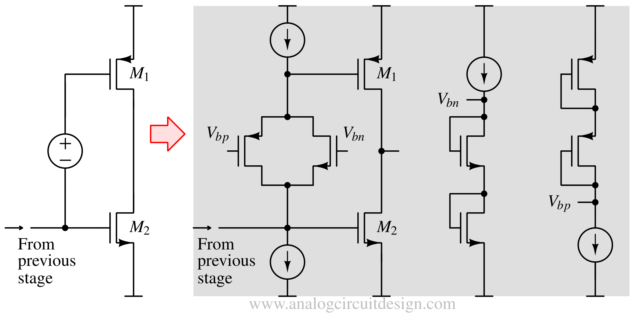
Nested miller compensation

Nested Miller compensation technique is used in three-stage or higher-stage op-amps to ensure stability. It extends the traditional Miller compensation by adding compensation capacitors from output of each gain stage to final output. The condition to obtain overall 60° phase margin :
$$\cfrac{g_{m3}}{C_L}>2\cfrac{g_{m2}}{C_{M2}}>4\cfrac{g_{m1}}{C_{M1}}$$
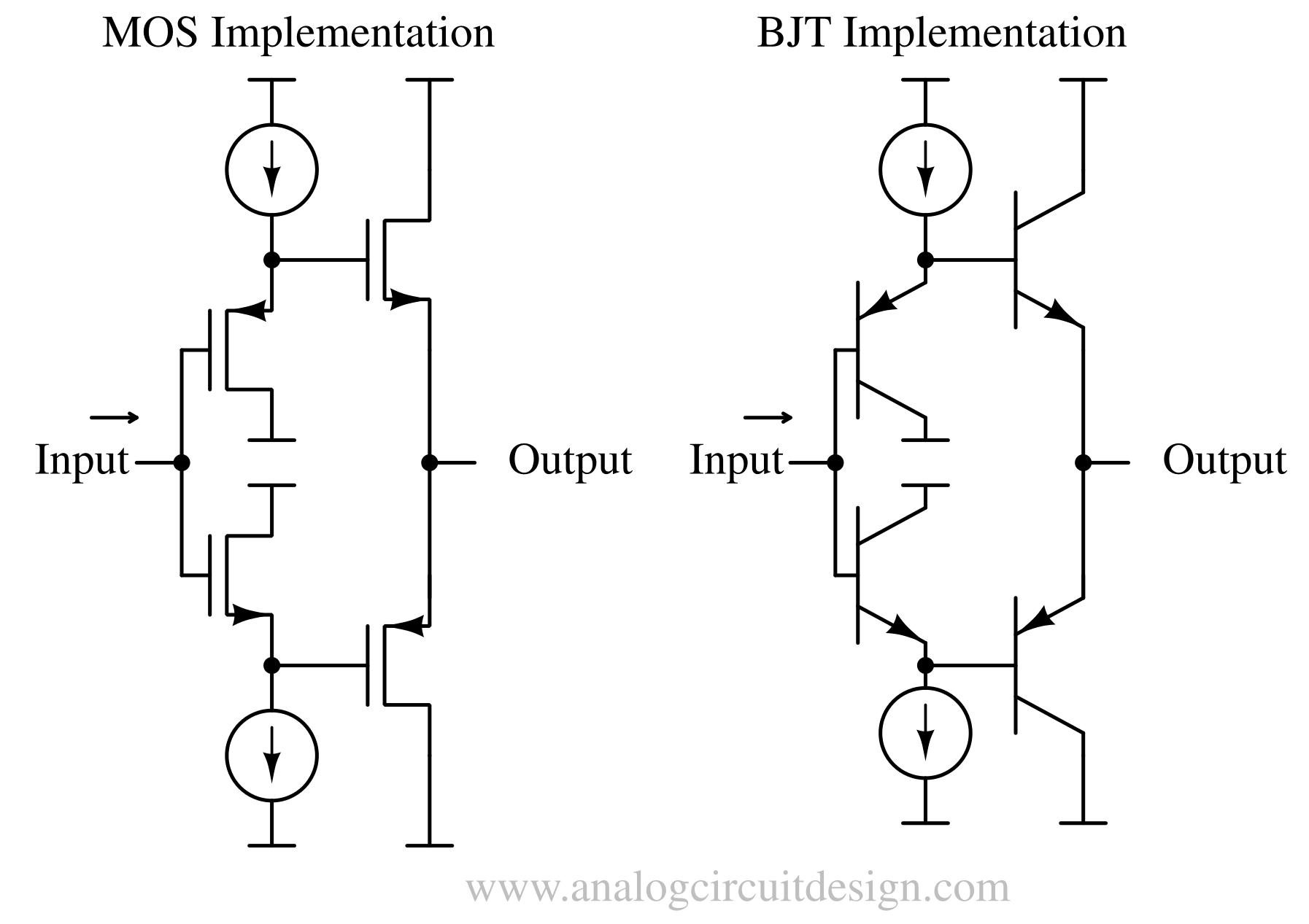
Feedforward or pole-zero compensation

To obtain same bandwidth and stability (phase and gain margin), the nested miller compensation can demand more power. This problem can be solved by using the Feedforward compensation scheme.
Types of input stage cascodes
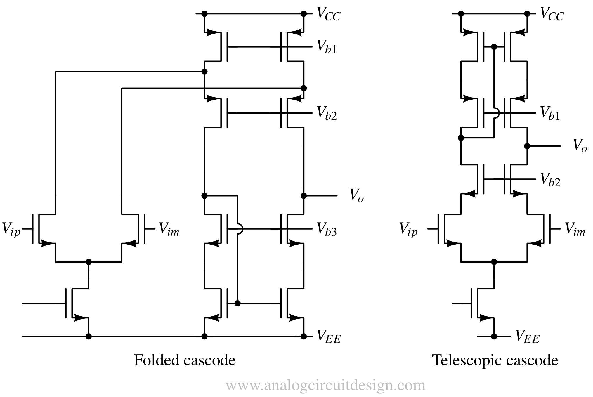
Telescopic cascode
A telescopic cascode is a high-gain amplifier topology commonly used in operational amplifiers and analog integrated circuits. It employs cascoded transistors stacked vertically to significantly increase output resistance and achieve very high voltage gain. However, this topology requires substantial voltage headroom, limiting output swing and making it less suitable for low-supply-voltage designs. For low supply voltage or input signals near supply voltages, folded cascode is used instead.
For a NPN/NMOS input differential pair, the cascode transistors are also NPN/NMOS as shown in figure above.
Folded cascode
A folded cascode is a high-gain amplifier topology commonly used in operational amplifiers to overcome the voltage headroom limitations of telescopic cascodes. In this architecture, the signal current from the input differential pair is “folded” into a different voltage domain. Folded cascodes provide better output swing for the same output resistance than telescopic designs. However, they consume more power due to additional branches and introduce additional noise due to extra devices.
For NPN/NMOS input differential pair, the cascode transistors are PNP/PMOS as shown in figure above. The signal from NMOS differential input pair is folded to the common-gate transistor.
Pro design tip
In a folded cascode transistor, we keep the current in main differential input high (to achieve high gm) and the cascode branch low. To achieve higher slew-rate, a parallel slew-boost circuit is added. The slew-boost circuit is a class AB circuit which dynamically increases the current during slew.