P-Channel MOSFET (PMOS)
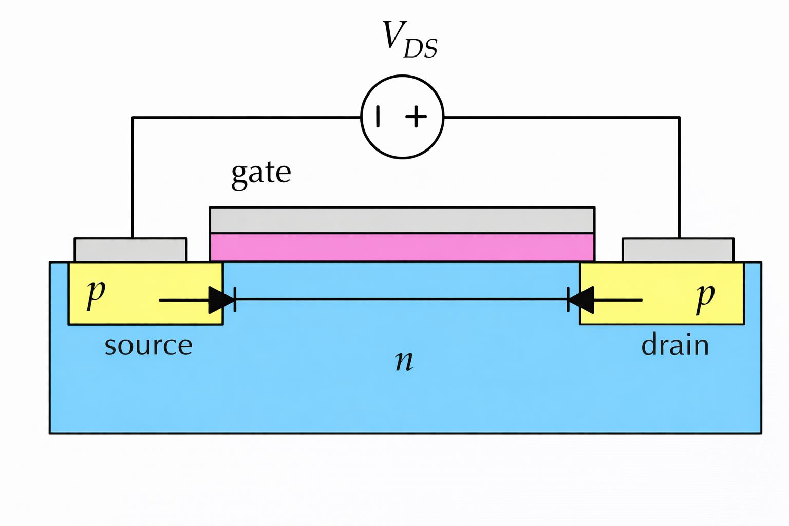
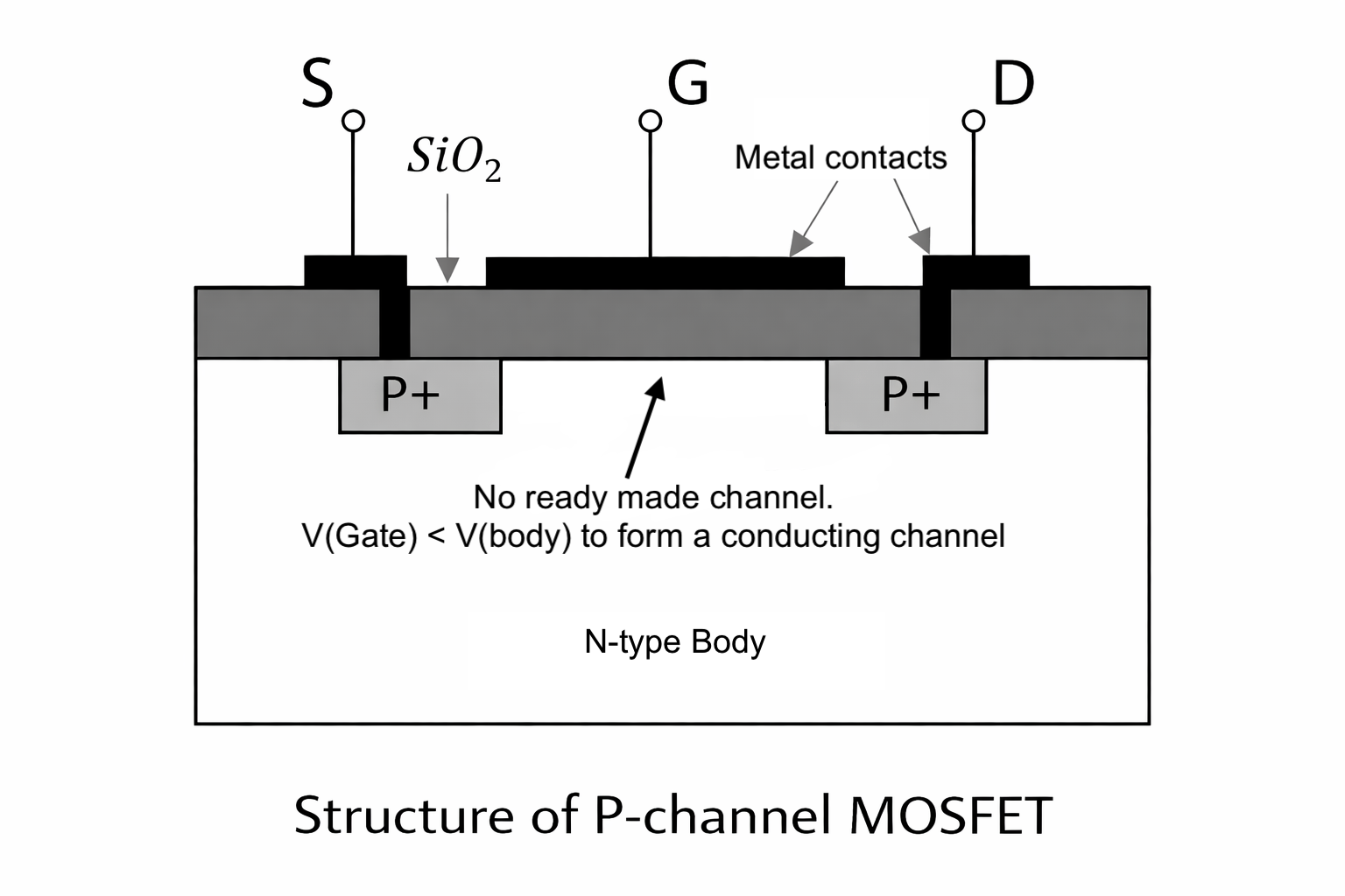
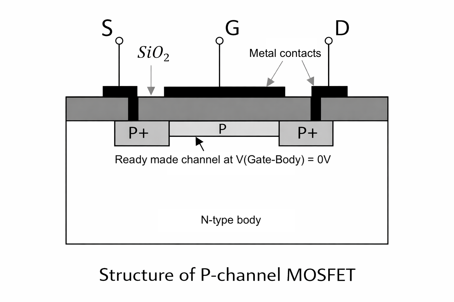
PMOS stands for P-channel metal-oxide-semiconductor. The structure of a PMOS transistor consists of three main regions: a P-type source, a P-type drain, and an N-type body (or well). The current flows through a P-type channel formed under the gate-oxide between the source and drain in the N-type body. The Gate is separated from the body using a thin oxide SiO2.
PMOS symbol
There are multiple symbols representing a P-channel MOSFET as shown below. These symbols are used in different domains of electronics. The body arrow symbol is popular in power electronics and discrete domain. The source arrow symbol is popular in signal chain and IC design domain. The circle at the gate is popular in digital electronics.
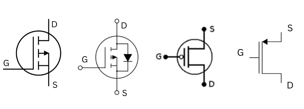
The body arrow always points from the P-type material to the N-type material. In a P-channel device, the channel is P-type and the substrate (body) is N-type, so the arrow points outward from the channel. If the arrow is shown at the source terminal, it indicates the direction of current flow when the device in turned on. Arrow is never shown at the drain terminal as drain terminal does not control the current flow.
There are minimum three terminals in a PMOS : Gate, Source and Drain. Most of the symbols assume Source and body shorted. Otherwise there is another terminal called Body. In integrated circuit designs, the n-type body (or N-well) is diffused in a p-type substrate. This substrate can be tapped using another terminal called substrate.
In many discrete MOSFET symbols, an internal parasitic diode is shown pointing from the drain to the source for P-channel devices.
PMOS vs NMOS differences
Key differences between a PMOS and a NMOS are tabulated below :
| Parameter | P-Channel | N-Channel |
|---|---|---|
| Carrier Type | Holes | Electrons |
| Turn ON Condition | Gate voltage is lower than source (VG < VS) | Gate voltage is higher than source (VG > VS) |
| Body Connection | Connected to most positive voltage (VDD) | Connected to most negative voltage (VSS or GND) |
| Mobility of Carriers | Lower (hole mobility) | Higher (electron mobility) |
| Switching Speed | Slower | Faster |
| Power Consumption | Generally higher when ON | Generally lower when ON |
| Size for Same Drive | Larger (to compensate for low mobility) | Smaller |
| Pull-up/down | Pull-up networks in CMOS logic | Pull-down networks in CMOS logic |
Operation of PMOS transistor
PMOS transistors starts conducting when a negative voltage is applied at the gate terminal while the source terminal is held at ground. When a positive voltage is applied to the gate terminal relative to the body, it creates an electric field that attracts holes (positive charge carriers) from the source region towards the gate. This electric field forms a conducting p-type channel ("inversion layer") between the source and drain. Once the channel is formed, applying a voltage across drain source leads to current flow through this channel. Usually, body is shorted to source or the highest potential available to avoid additional voltage source.
In PMOS transistors, the majority carriers are holes, and the flow of current occurs when the gate voltage is lower than the source voltage (in a common configuration known as enhancement mode). When the gate voltage is higher than the source voltage, the transistor is turned off.
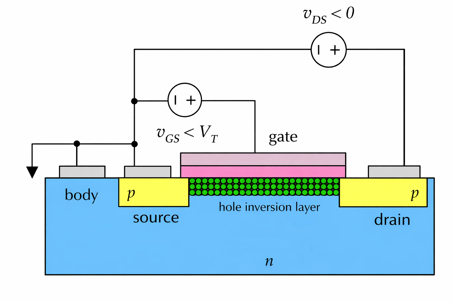
Importance of channel inversion

Without hole inversion layer underneath the gate oxide (VGS=0), there is always a reverse biased diode blocking current flow when a VDS is applied. With channel inversion, there is a parallel path which conducts current.
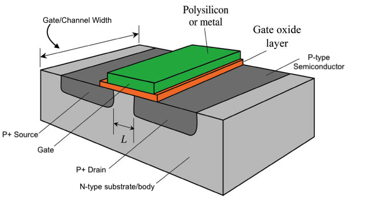
Construction of PMOS Transistor
The cross-section of a PMOS transistor typically consists of substrate, source, drain, gate, and channel regions.
Each component is described below:
Substrate
The substrate is typically p-type semiconductor material (e.g., silicon). The connection to this P-substrate is done using p+ doping called PSUB. An N-well is formed where the actual PMOS device resides. It provides the foundation for the PMOS structure. The substrate is connected to the lowest voltage potential in the circuit.
Source and Drain Regions
On the surface of the substrate, there are two heavily doped p-type regions known as the source and drain. These regions are created by introducing impurities (e.g., boron) into the well through a process called diffusion.
Channel Region
A thin layer of p-type carriers is located near the surface between the source and drain region in the n-type substrate when the gate voltage applied is less than the source voltage. Since the carrier type changes from n-type to p-type near the surface of the substrate, this process is called "inversion".
Gate (Control terminal)
Above the channel region is a thin insulating layer (usually silicon dioxide) followed by a metal gate electrode. The gate controls the conductivity of the channel by applying a voltage.
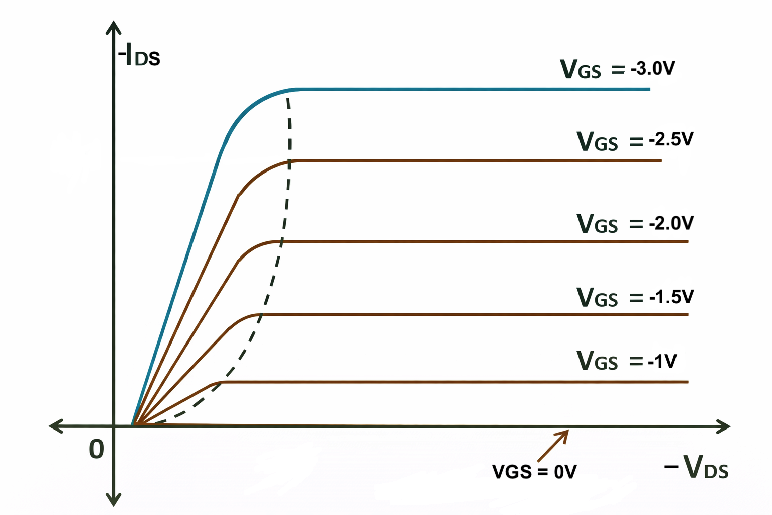
PMOS Transistor current-voltage relationship
PMOS transistor in the triode region behaves as a voltage-controlled resistor (similar derivation as done in NMOS). The relation of drain-source current with gate-source and drain-source voltage for a enhancement mode PMOS is given below:
$$I_{SD}=\mu{}_pC_{ox}\cfrac{W}{L}\left(V_{SG}-V_{TH}-\cfrac{V_{SD}}{2}\right)V_{SD}$$
PMOS transistor in the active region behaves as a current-controlled current source (CCCS):
$$I_{SD}=\cfrac{\mu{}_pC_{ox}}{2}\cfrac{W}{L}\left(V_{SG}-V_{TH}\right)^2(1+\lambda{}V_{SD})$$
The graph shown below represents the equation above :

PMOS capacitor
Channel formation results in the creation of a PMOS capacitor structure. The gate terminal functions as one conductive plate, while the induced channel region serves as the opposing plate, together forming an effective parallel-plate capacitance across the gate oxide insulator. The channel is accessed through the source and drain terminal shorted together.
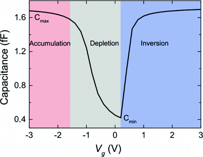
| Gate-body voltage | Region | Capacitance |
|---|---|---|
| VGB > 0 | Electron accumulation | Maximum capacitance |
| VT < VGB < 0 | Carrier depletion | Miniumum capacitance |
| VGB < VT | Inversion (sheet of holes form) | Maximum capacitance |
This capacitor is highly nonlinear. The capacitance value changes a lot with gate-bulk voltage.
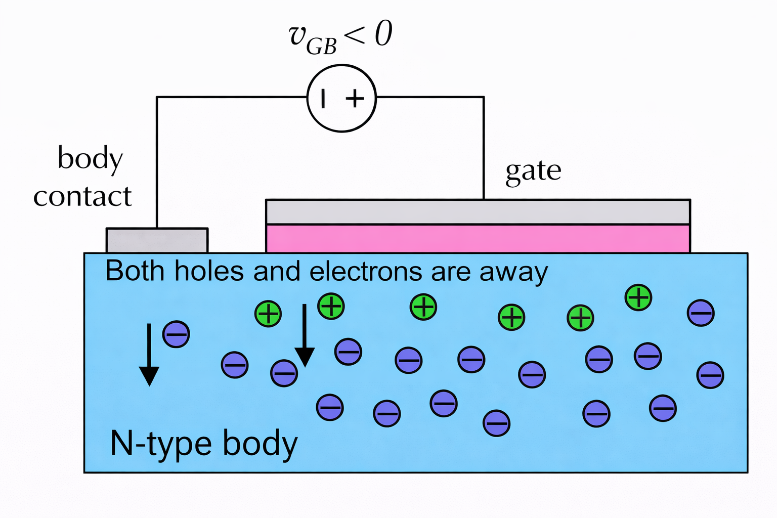
Accumulation region
A positive gate-to-body voltage attracts electrons from the n-type body toward the region beneath the gate oxide. The polysilicon gate acts as one plate of the gate capacitance, while the accumulated electron layer forms the opposing plate. This charge layer is electrically accessible through the body terminal. Access via the source and drain terminals is not possible because their p–n junctions remain reverse biased. The capacitance is maximum and equal to the oxide capacitance (Cox).
Depletion region
A slight negative or near zero gate-to-body voltage attracts holes towards the region beneath the gate oxide. These holes recombine with electrons leaving no charges near the surface (area below the gate oxide). Due to this depletion region, the distance between the equivalent parallel-plate capacitor increases. The capacitance is minimum at this point.
Inversion region
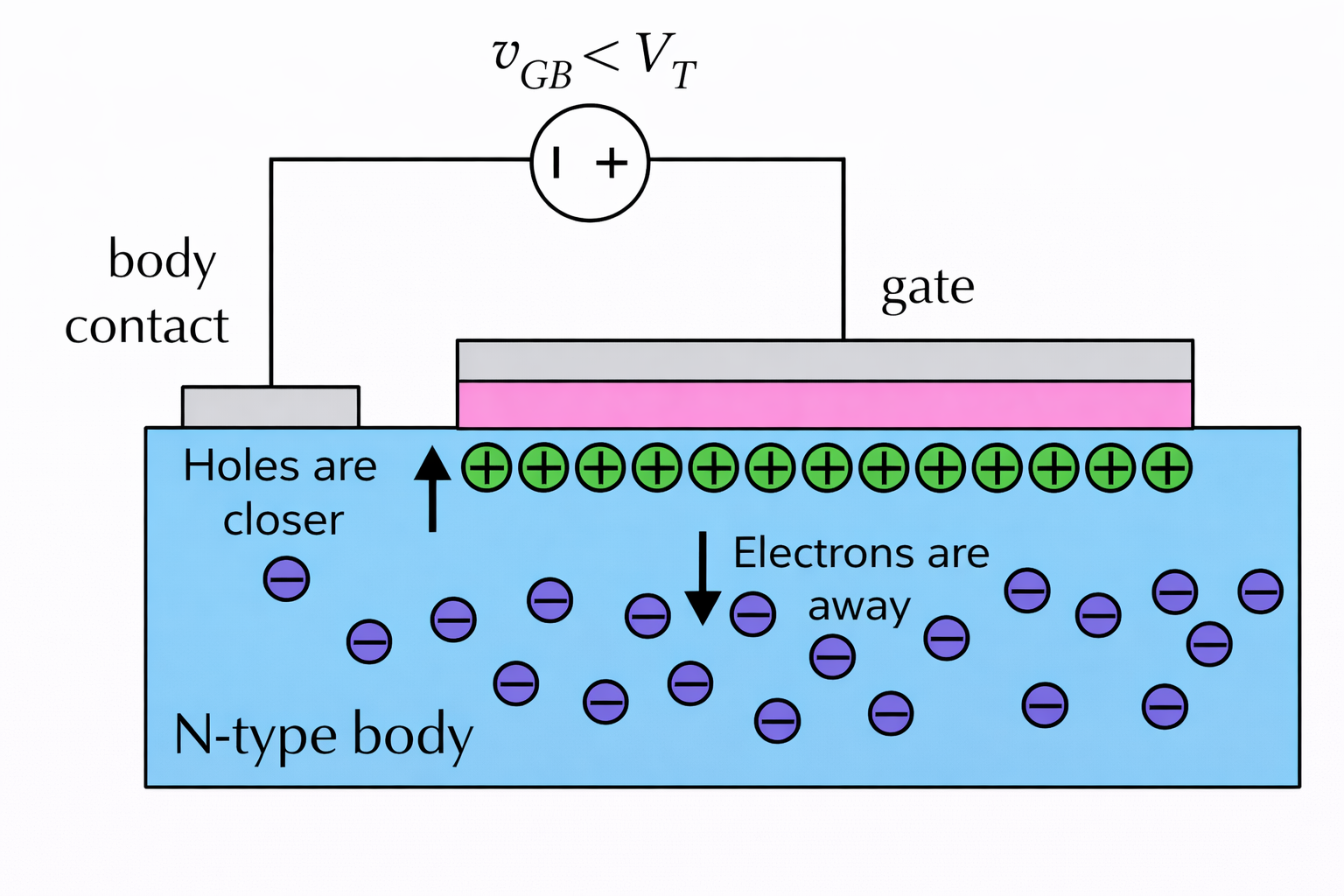
A strong negative gate-to-body voltage attracts holes from the n-type body and p-type source and drain toward the region beneath the gate oxide. The polysilicon gate acts as one plate of the gate capacitance, while the inverted hole layer forms the opposing plate. This charge layer is electrically accessible through the source and drain terminal. Access via the body terminal is not possible because the p–n junction is reverse biased. The capacitance is again maximum and equal to the oxide capacitance (Cox).
Enhancement and Depletion mode P-channel MOSFET
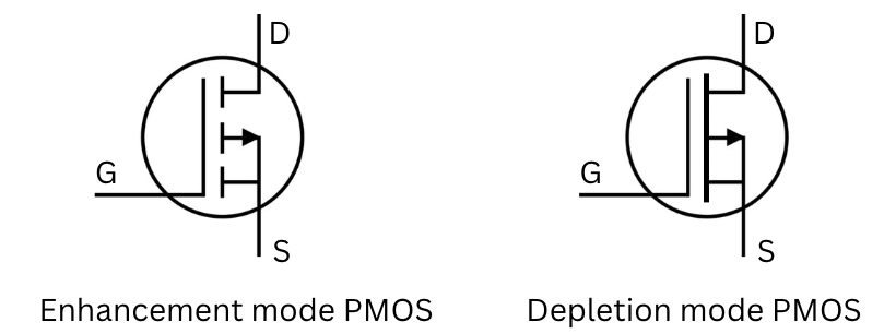
Enhancement Mode is represented by a dashed line between the drain and source, indicating the channel is not naturally formed and broken. Depletion Mode PMOS is represented by a solid line, indicating a built-in channel exists.
Enhancement mode P-channel MOSFET
The Enhancement Mode PMOS (Normally-OFF) is a three-terminal device consisting of the Source (S), Gate (G), and Drain (D) terminals. It does not have a pre-existing channel between source and drain. When a negative gate-to-source voltage (VGS) exceeding the threshold magnitude is applied, a channel is induced. Once formed, applying a negative drain-to-source voltage initiates conduction.
Case 1 (VGS=0) Since there is no channel formed, even with a negative VDS (or a positive VSD) there is no drain current ISD.
Case 2 (VGS<0) Minority carriers in the N-type substrate, namely holes, are attracted toward the gate terminal, creating the P-channel. This enhancement of channel charge raises the drain current, causing ( ISD ) to flow when a negative VDS is applied.
Case 3 (VGS>0) A channel of electron forms but is the part of reversed biased diodes. So, no conduction happens.
Depletion mode P-channel MOSFET
A P-channel depletion MOSFET (Normally-ON) is a three-terminal device similar to a P-channel enhancement MOSFET. The key distinction is that a P-type channel is already present at zero bias; otherwise, the structure and terminals remain the same.
A P-channel depletion MOSFET is structurally analogous to an N-channel depletion device; the primary difference lies in the polarity of the applied terminal voltages and resulting current directions. Because the channel is pre-formed, unlike in an enhancement-type MOSFET, a drain current flows even when the gate-to-source voltage is zero.
Case 1 (VGS=0) When a negative VDS is applied, holes from the pre-formed P-channel drift toward the drain terminal, initiating drain current ID. As the magnitude of VDS increases with VGS=0, the drain current saturates, where ID becomes constant and reaches maximum called IDSS.
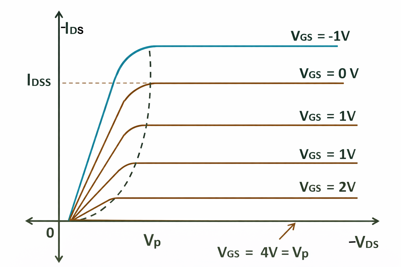
Case 2 (VGS>0) Electrons from the N-type substrate are attracted toward the positively biased gate and recombine with holes in the P-channel, reducing the available hole concentration. As the positive gate voltage increases, recombination intensifies, further depleting the channel and lowering ( ID ). Eventually, the drain current becomes zero. The gate voltage at which ( ID = 0 ) is defined as the pinch-off voltage ( VP ).
Case 3 (VGS<0) Minority carriers in the N-type substrate, namely holes, are attracted toward the gate terminal, increasing the hole concentration in the P-channel. This enhancement of channel charge raises the drain current, causing ( ID ) to exceed the zero-bias saturation current.
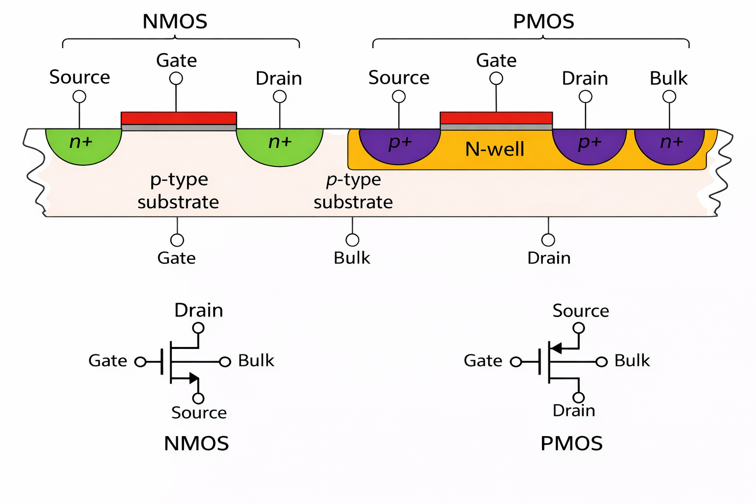
PMOS in CMOS technology
PMOS transistors are commonly used in complementary metal-oxide-semiconductor (CMOS) technology, where they are paired with NMOS (N-channel MOS) transistors to create digital logic circuits. CMOS technology allows for low power consumption and high noise immunity, making it widely used in integrated circuits and microprocessors.
PMOS as a switch
A PMOS transistor functions effectively as a switch in digital and analog circuits, particularly in logic gate design and high-side switching applications. It turns ON when the gate voltage is lower than the source (typically when the gate is at logic ‘0’), allowing current to flow from source to drain. Conversely, it turns OFF when the gate voltage is HIGH (logic ‘1’), creating a open (high-impedance) that blocks current flow. This complementary behavior to NMOS makes PMOS ideal for use in CMOS (Complementary MOS) logic circuits, where it typically forms the pull-up network.

Summary
- PMOS is built with a p-type source and drain and an n-type substrate.
- PMOS, carriers are holes.
- When a high voltage is applied to the gate, PMOS will not conduct
- When a low voltage is applied in the gate, PMOS will conduct.