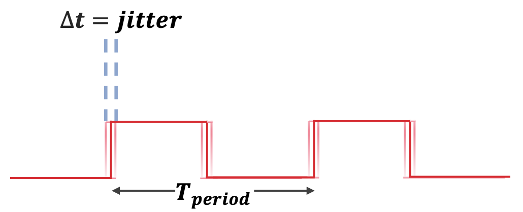
Clock Jitter
Clock Jitter or Jitter is defined as the local and rapid variations of a clock generators (oscillators) time periods from their ideal positions in time domain. Timing variations that occur slowly (more than 100x time-period) are called wander or drift, whereas jitter describes more rapid variations. It is directly related to Phase noise.
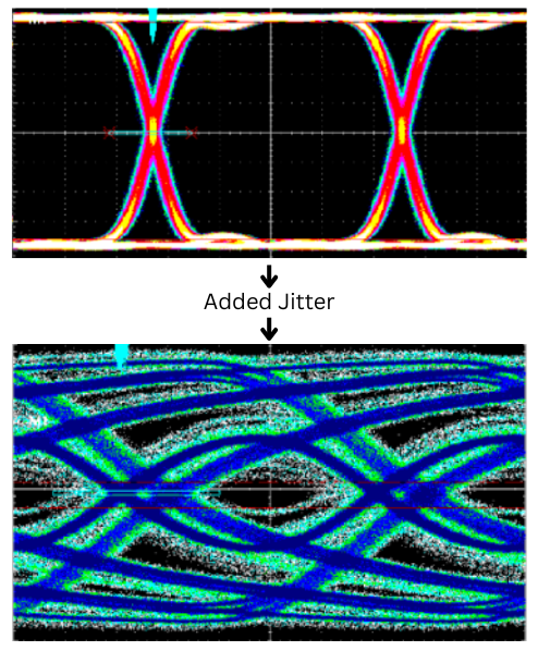
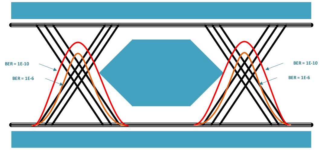
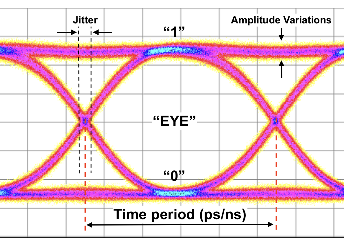
When noise, interference, or losses are introduced into a signal, the eye diagram shows a reduced eye opening, which leads to an increased bit-error rate (as illustrated below).
The main factors causing jitter are device noise, power supply variations, loading conditions, device noise, and interference coupled from nearby circuits.
Relationship between Phase-noise and Jitter
$$J_{RMS}=\sqrt{\int_{f_L}^{f_H}S_{\Delta{}t}(f)df}=\cfrac{1}{2\pi{}f_0}\sqrt{\int_{f_L}^{f_H}S_{\phi{}}(f)df}$$
Here, JRMS is Root mean square jitter having units as seconds. Sφ(f) is the phase noise power spectral density (PSD).
Derivation : Phase noise to Jitter transformation
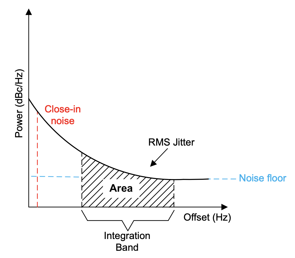
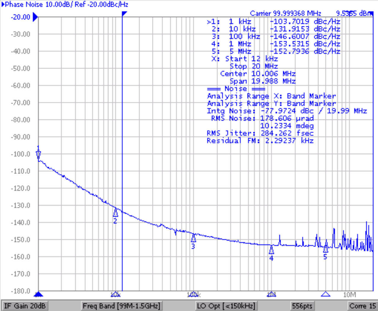
Usually, the phase noise is provided as a plot as shown above. Since, it is in dBc/Hz, it has to be converted into radians first by taking anti-log. Using the following formula, we can obtain the jitter:
$$J_{RMS}=\cfrac{\sqrt{2*10^{Area/10}}}{2\pi{}f_0}$$
Jitter Representation and Interpretation
Clock jitter can be represented in many ways :
Period jitter
Time difference between real clock period and ideal clock period. In reality, there is no ideal clock so this ideal clock period is the mean clock period over a certain number of periods.
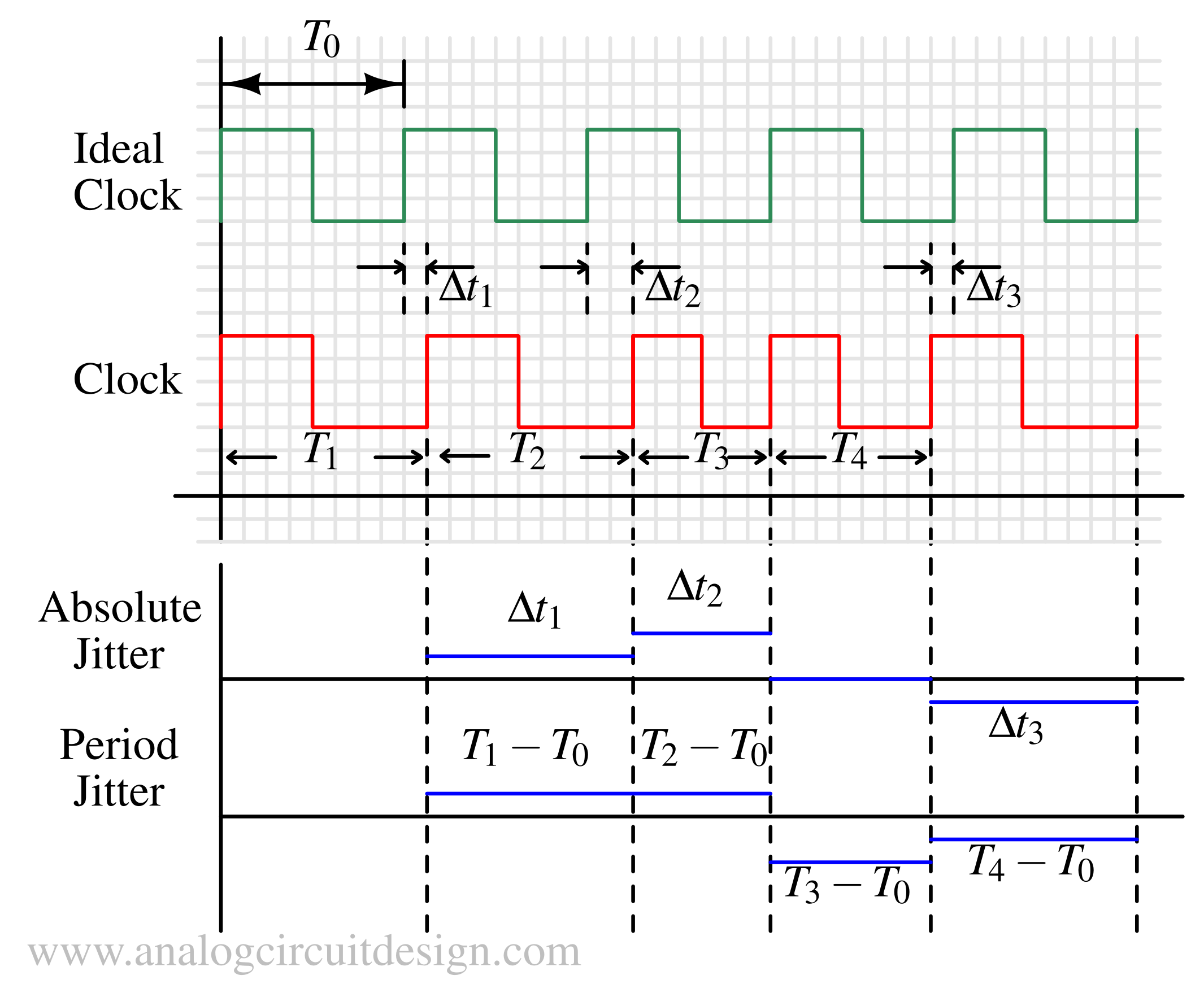
Absolute Jitter
Time difference between real clock edge and ideal clock's edge for the same cycle. The difference between Period jitter and Absolute jitter is illustrated above.
N-period jitter
Time difference between measured period and ideal period, measured over a specified number (N) of consecutive periods. Period Jitter is nothing but N-period jitter, when N=1.
Cycle-to-cycle jitter
Time difference between two adjacent clock periods. Cycle-to-cycle jitter is calculated by taking the difference of period jitter. Important for budgeting on-chip digital circuits cycle time.
It is also called short-term jitter because it does not hold meaningful value over long duration. Low cycle to cycle jitter does not mean a stable clock. This is because, for example, the cycle-to-cycle jitter may remain consistent while the frequency slowly drifts to half its original value.
Accumulated Jitter
Time difference between measured clock and ideal trigger clock. Jitter measurement most relative to high-speed link systems.
Jitter Statistical Parameters
Mean Value
Mean jitter be interpreted as a fixed timing offset or “skew". Generally not important, as usually can be calibrated out.
RMS Jitter
This represents the root-means-square jitter. It can be calculated from Phase noise. It is useful for characterizing random component of jitter.
Peak-to-Peak Jitter
Peak to Peak Jitter is a function of both deterministic (bounded) and random (unbounded) jitter components. Must be quoted at a giver BER to account for random (unbounded) jitter.
Types of Jitter
Jitter can be classified into following categories1 2:
flowchart TD
    A[Total Jitter] --> C[Random]
    A --> B[Deterministic]
    B --> D[Data Dependent Jitter, DDJ]
    B --> E[Sinusoidal or Periodic Jitter, PJ]
    D --> F[Bounded Uncorrelated Jitter, BUJ]
    D --> G[Intersymbol Interference, ISI]
    D --> H[Duty Cycle Distortion, DCD]
Total jitter is summation of all Deterministic and Random jitter.
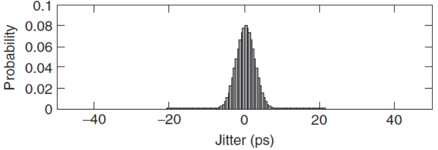
Random Jitter (RJ)
Random jitter is unbounded and unpredictable, and it follows a Gaussian distribution. Because a Gaussian distribution has infinite tails, the peak-to-peak value of random jitter is theoretically infinite, making peak-to-peak measurements meaningless. Instead, random jitter is characterized by its mean (\mu) and standard deviation (\sigma). Common sources include device noise (shot, flicker, and thermal noise), quantization error, reference clock jitter, and PLL jitter. Random jitter must always be specified together with a bit error rate (BER).
It can be mathematically represented as:
$$RJ(t)=\cfrac{1}{\sqrt{2\pi{}}\sigma_{RJ}}e^{-\cfrac{t^2}{2\sigma_{RJ}^2}}$$
Deterministic Jitter
Deterministic jitter is bounded and has a predictable peak-to-peak value; beyond a certain limit, its probability density function (PDF) becomes zero, indicating finite bounds. In contrast, the PDF of random jitter never reaches zero. Common sources of deterministic jitter include transmission-line losses, reflections, rise- and fall-time mismatches, spread-spectrum clocking, duty-cycle distortion, and crosstalk.
There are following categories of deterministic jitter (DJ):
- Sinusoidal or Periodic Jitter (SJ or PJ)
- Data Dependent Jitter (DDJ) :
- Intersymbol Interference (ISI)
- Duty Cycle Distortion (DCD)
- Bounded Uncorrelated Jitter (BUJ)
Sinusoidal or Periodic Jitter
Sinusoidal or Periodic jitter repeats at a fixed frequency due to modulation effects such as power-supply modulation, spread-spectrum clocking, or PLL reference clock feedthrough. It can be decomposed into a Fourier series of sinusoidal components as follows:
$$SJ(t)=\sum_{i}^{}A_i\cos(\omega{}_it+\theta_i)$$
The jitter produced by an individual sinusoid is :
$$PDF_{SJ}(t)=\begin{cases}\cfrac{1}{\pi{}\sqrt{A^2-t^2}} &\mbox{A>|t|} \\ 0 &\mbox{A<|t|} \end{cases}$$

Data Dependent Jitter (DDJ)
Data-dependent jitter is correlated with the transmitted data pattern or with aggressor data patterns in the case of crosstalk. It arises from effects such as phase errors in serialization clocks, channel filtering, and crosstalk. It has following categories:
- Duty cycle distortion (DCD)
- Intersymbol interference (ISI)
- Bounded Uncorrelated Jitter (BUJ)
Duty Cycle Distortion (DCD)
Duty cycle distortion is caused by duty-cycle errors in transmitter serialization clocks and by rise/fall delay mismatches in post-serialization buffers. The resulting probability density function (PDF) from a peak-to-peak duty cycle distortion αDCD is the sum of two delta functions, as shown below:
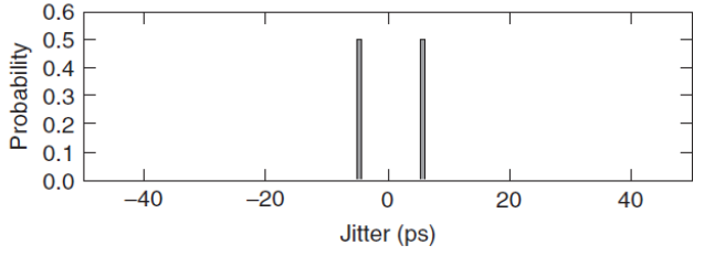
$$PDF_{DCD}(t)=\cfrac{1}{2}\left[\delta{}\left(t-\cfrac{\alpha{}_{DCD}}{2}\right)+\delta{}\left(t+\cfrac{\alpha{}_{DCD}}{2}\right)\right]$$
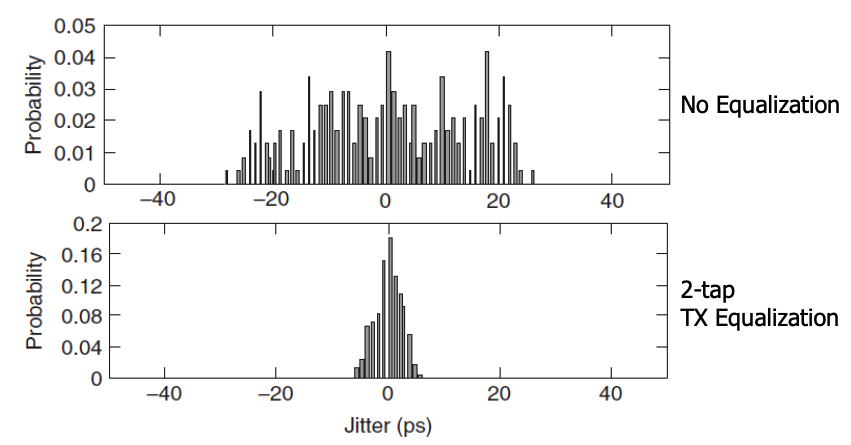
Intersymbol interference (ISI)
Intersymbol interference (ISI) is caused by channel loss, low-bandwith, dispersion and reflections. ISI can be improved by Equalization as shown below:
Bounded Uncorrelated Jitter (BUJ)
Bounded uncorrelated jitter is not aligned in time with the data stream. Its most common sources are crosstalk and substrate coupling3. It is correlated with aggressor signals rather than the victim signal, and although uncorrelated with the data stream, it remains a bounded jitter source with a quantifiable peak-to-peak value.
Total Jitter (TJ)
The total jitter PDF is produced by convolving the random and deterministic jitter PDFs.
$$PDF_{JT}(t)=PDF_{RJ}(t)*PDF_{DJ}(t)$$
Since, Total Jitter consists of both deterministic and random components, it must be quoted at a given BER.
Jitter can be visualized in a Eye pattern or Eye diagram as shown below : 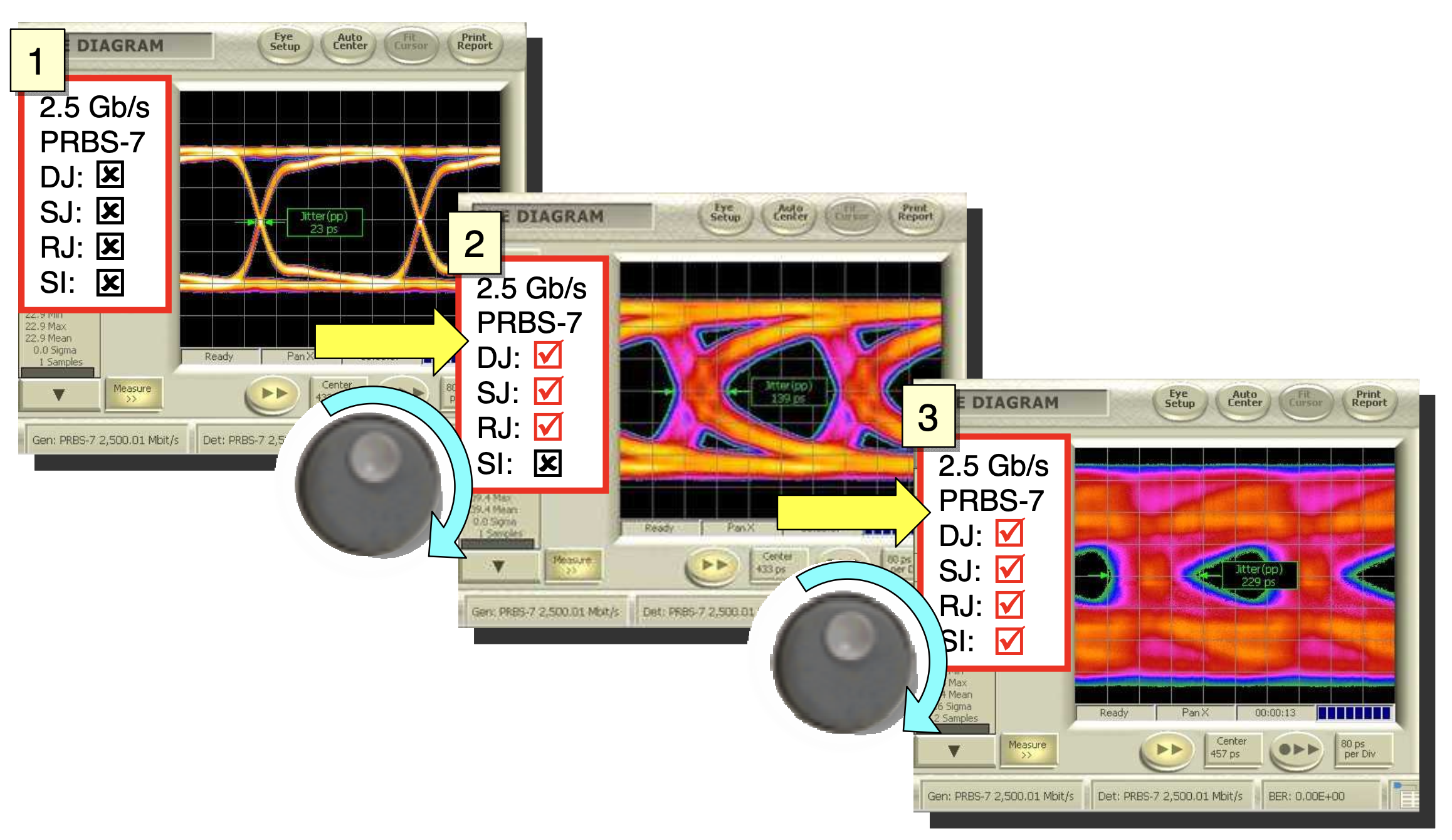
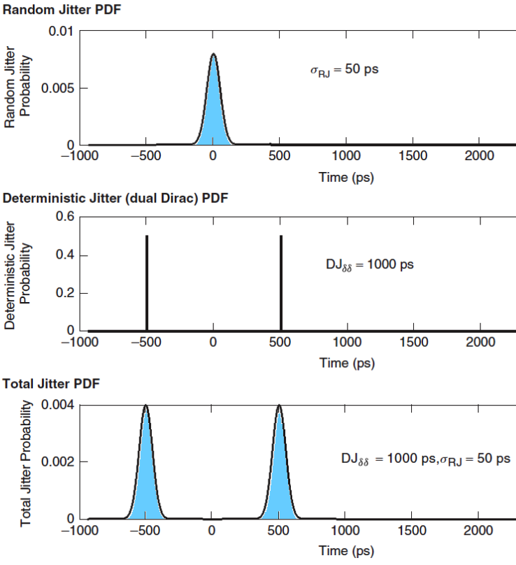
Dual Dirac Jitter Model
For system-level jitter budgeting, the dual-Dirac model enables separate allocation of deterministic and random jitter components.
Random jitter model:
$$RJ(t)=\cfrac{1}{\sqrt{2\pi{}}\sigma_{RJ}}e^{\cfrac{-t^2}{2\sigma_{RJ}^2}}$$
Deterministic jitter (duty cycle jitter) model:
$$DJ(t)=\cfrac{1}{2}\left[\delta{}\left(t-\cfrac{\alpha{}}{2}\right)+\delta{}\left(t+\cfrac{\alpha{}}{2}\right)\right]$$
Total Jitter,
$$TJ(t)=RJ(t)*DJ(t)=\cfrac{1}{2\sqrt{2\pi{}}\sigma_{RJ}}\left[e^{-\cfrac{t-\alpha{}/2}{2\sigma_{RJ}^2}}+e^{-\cfrac{t+\alpha{}/2}{2\sigma_{RJ}^2}}\right]$$
Jitter Debug and Mitigation
Common Jitter Sources and mitigations are :
| Source | Cause Description | Mitigation / Solution |
|---|---|---|
| External radiation | Interference caused by external electromagnetic sources | Use a Faraday cage to isolate the problem |
| Crosstalk / Adjacent trace transients | Coupling between neighboring signal traces | Requires shielding; must be addressed at the PCB design stage |
| Power supply coupling | Noise coupling through the power supply rails | Use an LDO (sub-regulator) with high PSRR and good load regulation; add a ferrite bead and decoupling capacitors |
| PLL behavior | Tracking errors or overshoot in the PLL | Increase loop bandwidth or improve loop stability |
| Channel effects | Limited bandwidth, reflections causing ISI, skin effect, dielectric absorption, and path discontinuities | Tune equalization; use TDR to debug and locate path discontinuities |
| Driver imbalance | Rise/fall time asymmetry in the driver | Can cause duty-cycle jitter; improve driver symmetry |
| On-chip coupling | Substrate coupling inside the IC | Use substrate taps connected to the nearest low-impedance ground |
Jitter Measurement
There are following ways of measuring jitter :
Jitter measurement using Eye Diagram and Oscilloscopes
Jitter is the deviation of a signal’s actual transition time from its ideal position. In an eye diagram, jitter appears as horizontal eye closure. Greater jitter means wider spread of zero-crossings.
Jitter measurement using Eye diagram.
The following video explains the jitter measurement using eye diagram in oscilloscopes :
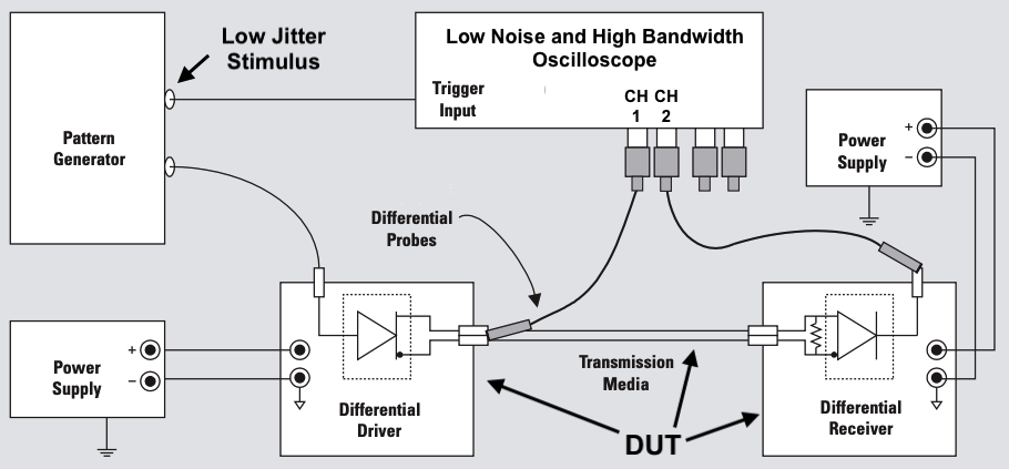
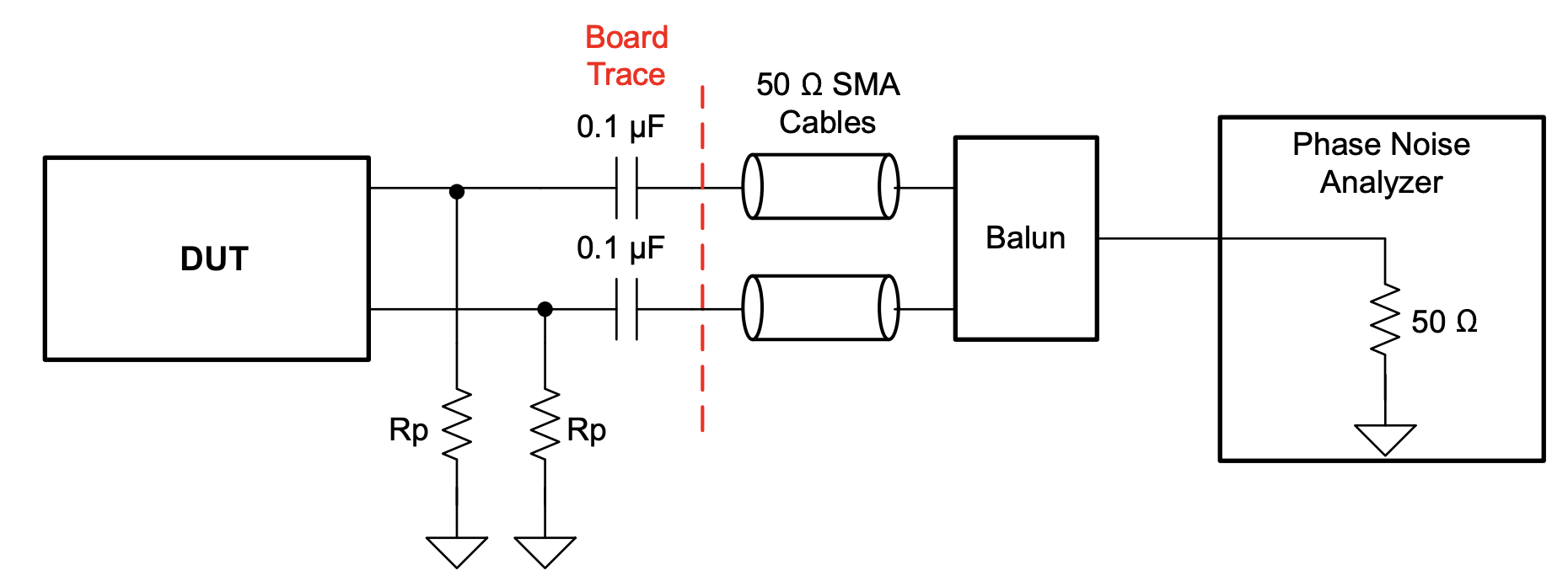
Jitter measurement setup
Jitter measurement using Phase noise analyzer
Jitter Impact
Some common areas where jitter impacts :
- Audio converters
- Data converters
- Clock and Data recovery
- Synchronous digital circuits
-
M. P. Li, Jitter, Noise, and Signal Integrity at High-Speed. Upper Saddle River, NJ, USA: Prentice-Hall ↩
-
Understanding Jitter and Phase Noise: A Circuits and Systems Perspective ↩
-
A. Tasic and W. A. Serdijn, "Effects of substrate on phase-noise of bipolar voltage-controlled oscillators," 2002 IEEE International Symposium on Circuits and Systems ↩