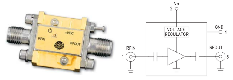
Low noise amplifiers (LNA)
A low-noise amplifier (LNA) is a special electronic signal amplifier that boosts very weak signals while adding minimal noise, thereby preserving the incoming signal's signal-to-noise ratio (SNR). It is primarily used at the front end of RF and wireless receiver chains, where incoming signals typically have very low SNR.
LNA architectures
LNAs are typically designed with a 50 Ω input resistance and minimal input reactance. This requirement decides LNA architecture2. The gain stage is made using a single transistor with inductive loading. Cascodes are added to provide better reverse isolation.

Cascode-type LNA with inductive degeneration
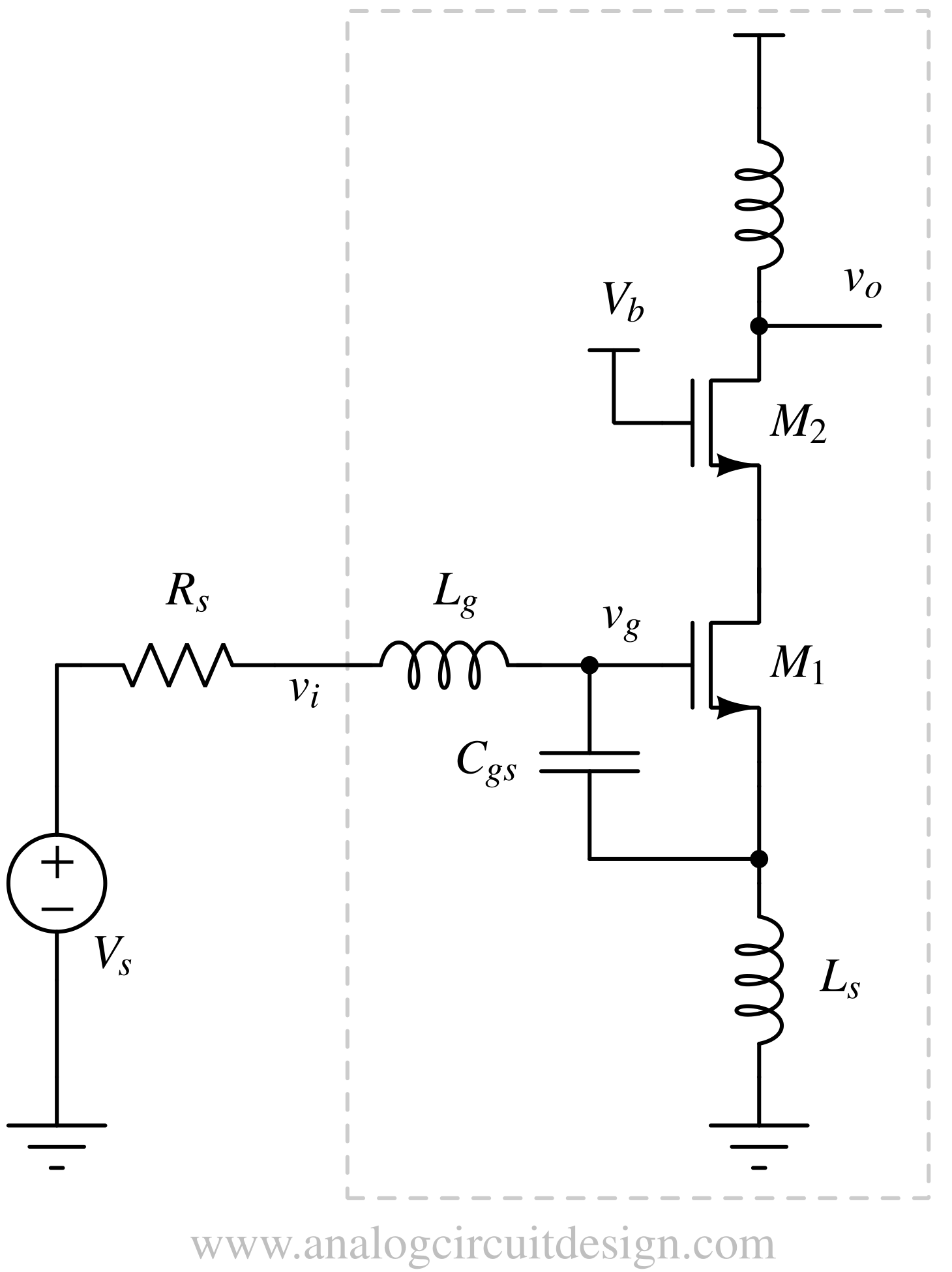
The cascode type LNA with inductive degeneration is the most popular narrow-band topology because it offers best noise figure while matching the input. Cascoding helps achieving high reverse isolation4.
Important LNA parameters
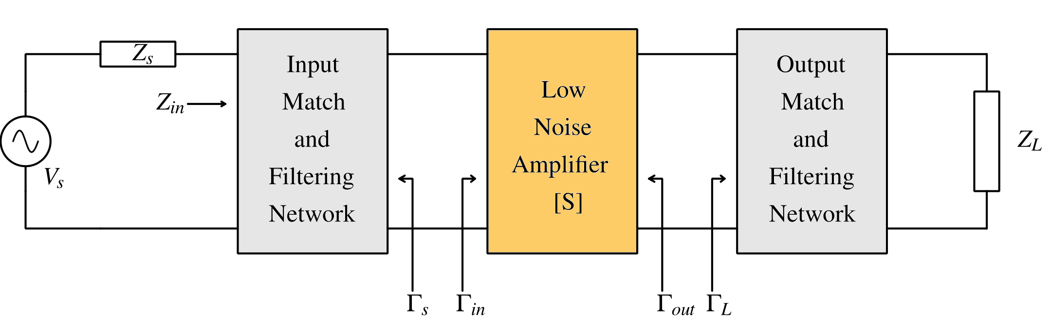
Amplifier S-matrix
$$[S]=\begin{bmatrix}s_{11} & s_{12} \\ s_{21} & s_{22}\end{bmatrix}$$
Input matching
Input matching is required to achieve maximum power gain and avoid reflections. In addition, preceding transmission line need a 50Ω termination to operate correctly. Proper matching also allows the LNA to be connected to an antenna at an unknown distance without concern for the transmission line length.
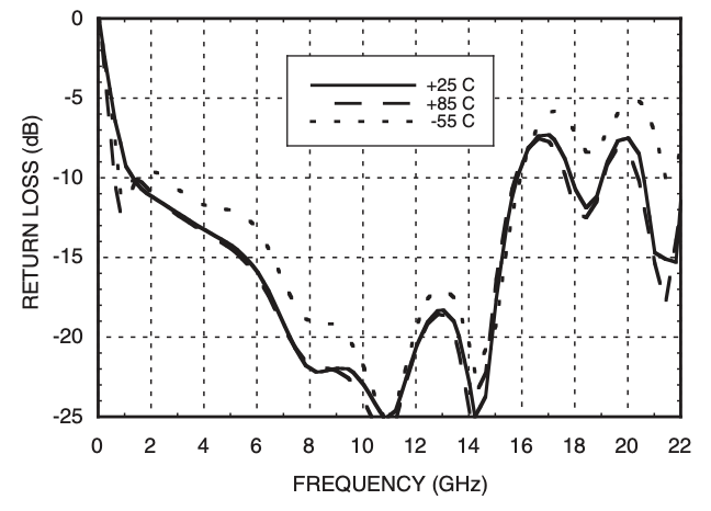
Return loss
Return loss indicates how of the incident signal is reflected back. Ideally, return loss should be zero. It is represented by reflection coefficients.
Input reflection coeffcient
$$\Gamma{}_{in}=s_{11}+\cfrac{s_{12}s_{21}\Gamma{}_L}{1-s_{22}\Gamma{}_L}$$
Γin is the input reflection coefficient and represents input return loss. It equals s11 if ΓL is zero (load is matched). ΓL is the load reflection coeffcient.

Output reflection coeffcient
$$\Gamma{}_{out}=s_{22}+\cfrac{s_{12}s_{21}\Gamma{}_S}{1-s_{11}\Gamma{}_S}$$
Γout is the output reflection coefficient and represents output return loss. It equals s22 if ΓS is zero (Source is matched). ΓS is the source reflection coeffcient.
Noise
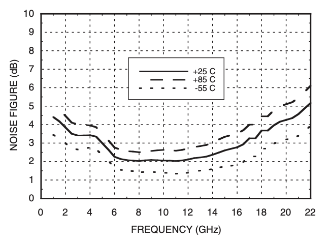
Noise factor is defined by the ratio of output SNR and input SNR. It shows the degradation of signal's SNR due to the circuits that the signal passes through. Noise figure is the dB form of noise factor.
Noise factor of cascaded system
An RF receiver signal chain consists of a cascaded set of components, with the antenna and LNA positioned at the front end.
$$F_{total}=F_{LNA}+\cfrac{F_{postLNA}-1}{Gain_{LNA}}$$
The LNA’s noise factor directly contributes to the overall system noise factor, while its gain reduces the impact of noise from subsequent stages.
Noise figure of basic LNA
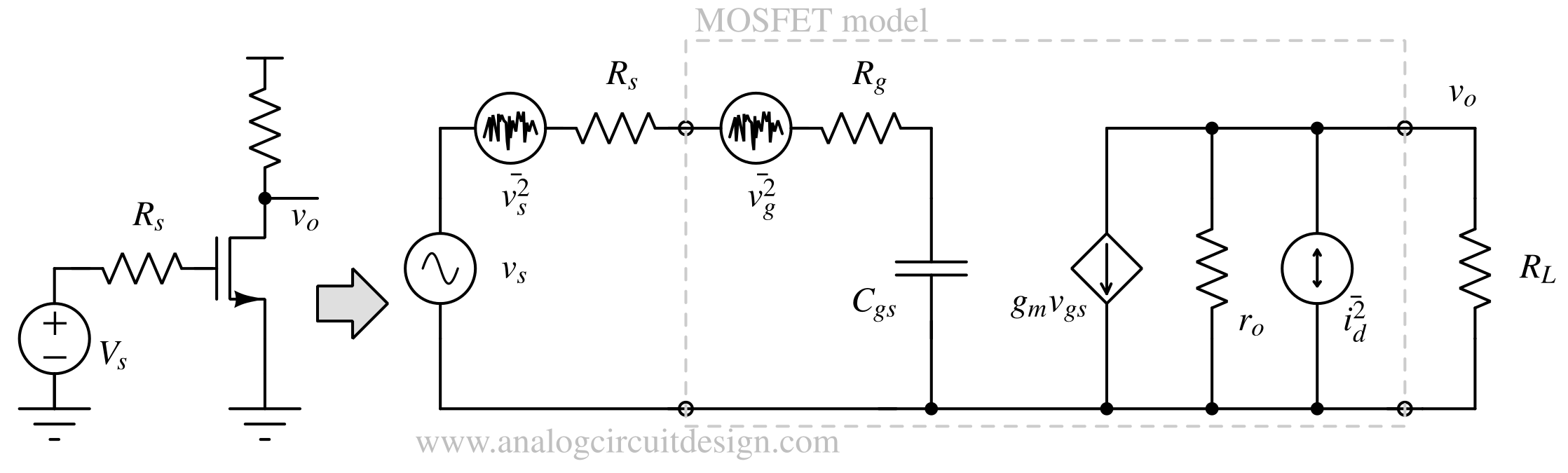
$$\text{F}=1+\cfrac{R_g}{R_s}+\left(\cfrac{\gamma{}}{\alpha{}}\right)\left(\cfrac{\omega{}}{\omega{}_T}\right)^2g_mR_s$$
For long channel MOS devices, γ=2/3 and α=1. γ is the noise modeling factor in: $$\bar{i_d}^2=4kT\gamma{}g_m$$
ωT is transistor's unity gain bandwidth. Rg is the distributed gate resistance which can be reduced by increasing the number of fingers. The above LNA architecture is not matched for a transmission line at the input. Matching the input for transmission lines poses limitation of achievable noise figure. These are discussed in LNA architecture section.
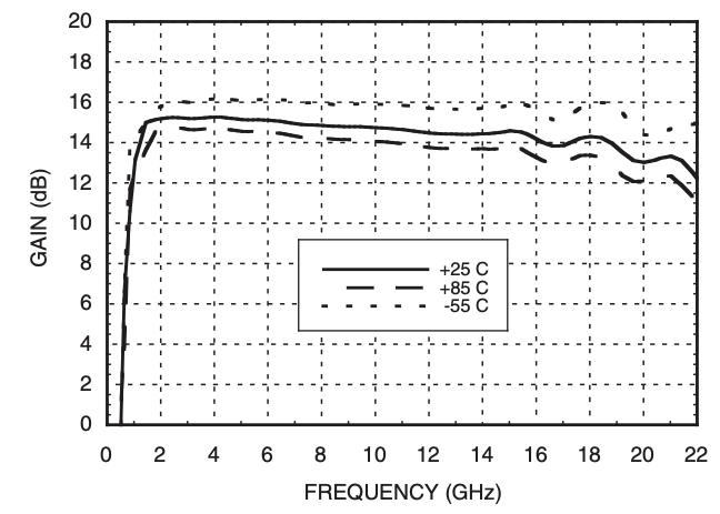
Gain
Gain is used to amplify signals which helps to reduce input referred noise of he subsequent stages. This gain is the small signal gain of the amplifier. It is represented by s-parameter s21. For integrated circuit implementation, the input of the LNA is interfaced off-chip and usually matched to 50 Ω impedance. Its output is necessarily not matched if directly interfacing inside the integrated circuit to a load (e.g., input of mixer or a filter).
Power gain
For a unilateral device (s12=0) power-gain is defined as power delivered to the load divided by the power available from source.
$$G_T=\cfrac{1-|\Gamma{}_S|^2}{|1-s_{11}\Gamma{}_S|^2}|s_{21}|^2\cfrac{1-|\Gamma{}_L|^2}{|1-s_{22}\Gamma{}_L|^2}$$
Linearity
The system's DC-transfer function can be modeled as :
$$Y_t=a_0+a_1X_t+a_2X_t^2+a_3X_t^3$$
If two strong slightly out of band inteferers appear at the LNA input, intermodulation distortion (3rd order nonlinearity) comes inside the band as shown below:
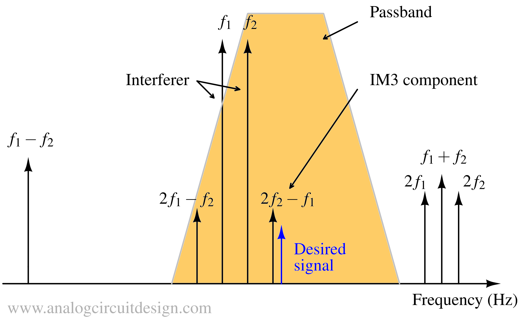
These large in-band blocker can desensitize the circuit.
Two-tone test is deployed to measure intermodulation distortion. Interferer can be modeled as :
$$X_t=A_1\cos(\omega{}_1t)+A_2\cos(\omega{}_2t)$$
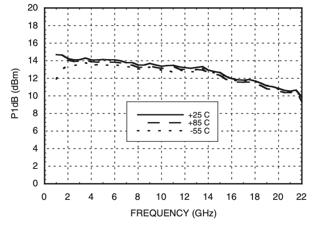
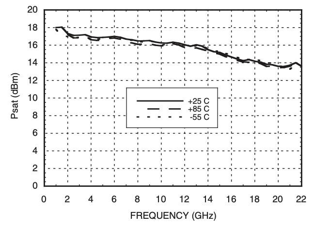
P1dB and Psat
The third order nonlinearity is compressive in nature because the output cannot go beyond supply voltage (or 2X of supply voltage is case of inductive load). Mathematically, compression happens when the third-order coefficient is negative when the linear coefficient in positive (a3a1 < 0).
P1dB is the output power when the amplifier is at the 1 dB compression point.
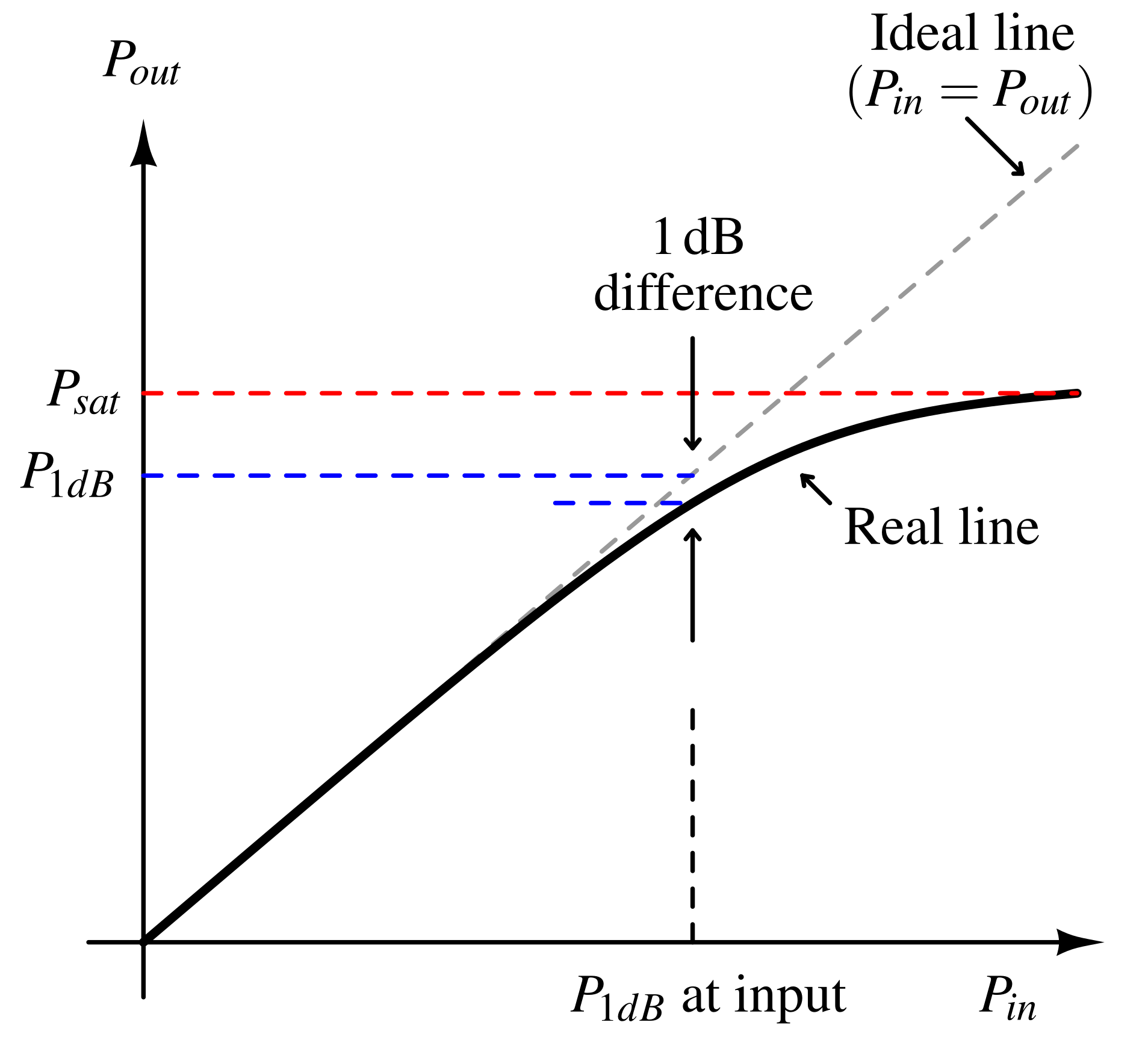
As shown in the graph above, the P1dB is measured by plotting output power vs input power and marking the point when the real curve is 1dB away from the ideal curve.
Psat is the output power when the amplifier is saturated. The output stops changing with increase in input power.
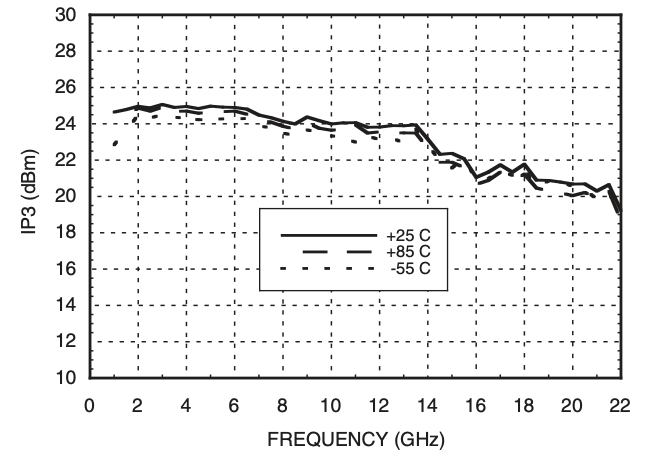
Output IP3 (OIP3)
The IP3 are indicators of good linearity of low noise amplifier. When the output of the low-noise noise amplifier is probed to measure IP3, it is called OIP3. When two-tone test is done, following fundamental and IM3 components are obtained :
Fundamental components
$$v_{fund}=a_1A_1+\cfrac{3}{4}a_3A_1^3+\cfrac{3}{2}a_3A_1A_2^2$$
If both amplitudes are equal,
$$v_{fund}=a_1A+\cfrac{9}{4}a_3A^3$$
The above term will compress when A starts becoming large. We will take only the linear extrapolated term for OIP3 calculation,
$$v_{fund}=a_1A$$
IM3 components
$$v_{im3}=\cfrac{3a_3A_1^2A_2}{4}$$
If both amplitudes are equal,
$$v_{im3}=\cfrac{3a_3A^3}{4}$$
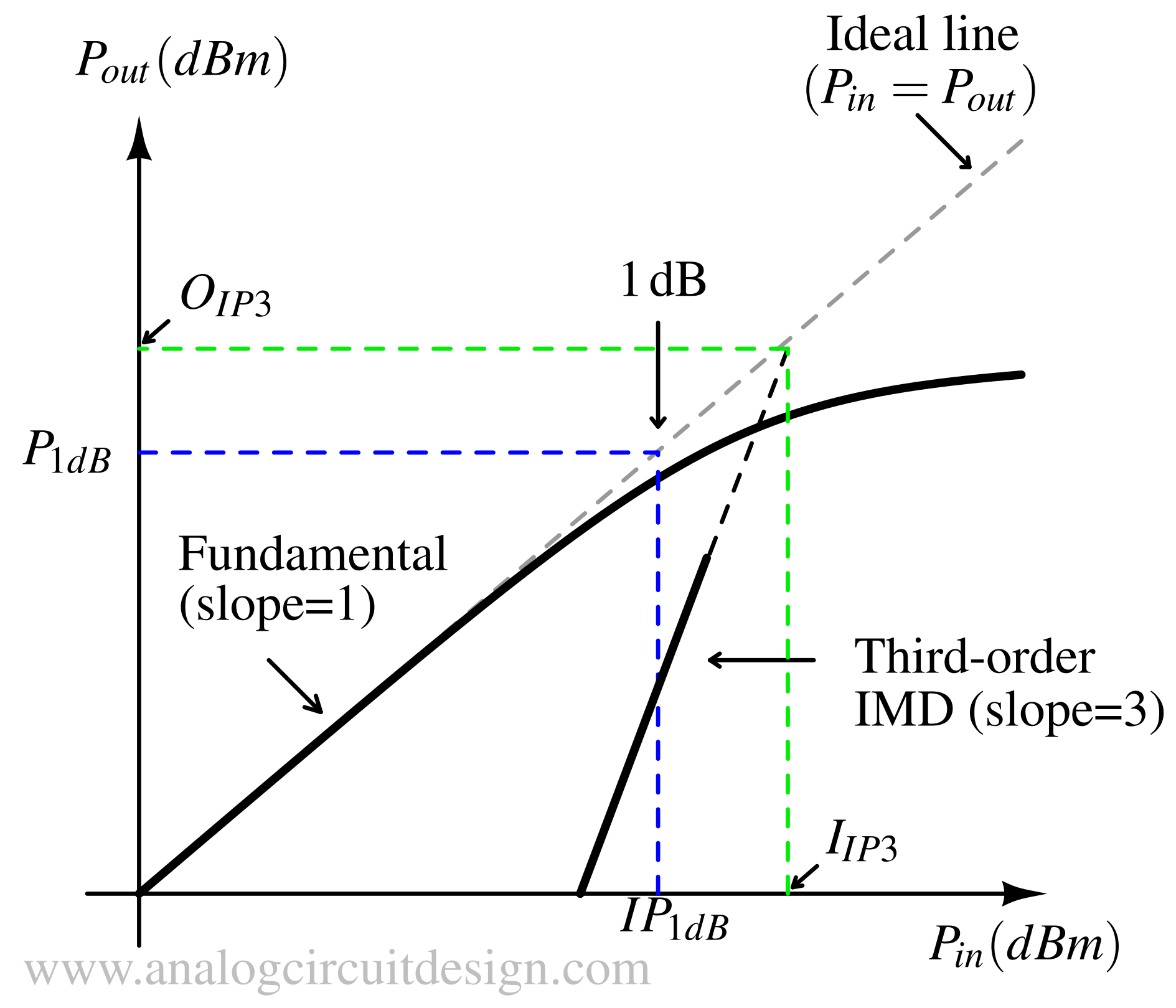
At lower amplitude, the fundamental component dominates over the IM3 products. However, at higher amplitudes, the IM3 components grow to become equal to or even exceed the fundamental amplitude. The interection point is called IP3.
$$v_{im3}=v_{fund}$$
$$\implies{}A=\sqrt{\cfrac{4a_1}{3a_3}}$$
$$I_{IP3}=10\log_{10}\left(\cfrac{A^2}{R_0}\right)$$
The above amplitude is called output intermodulation intercept point. This is the input amplitude where the linear and intermodulation-3 distortion meet.
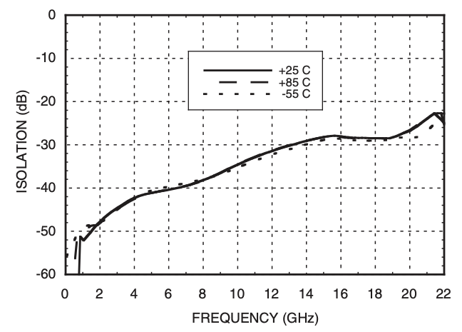
Reverse isolation
Reverse Isolation is a measure of the ability of an LNA to prevent signals from leaking or coupling back into its input port from its output port. In simpler terms, it quantifies how effectively an LNA isolates its output port from the input port. S12 of an LNA indicates reverse isolation. In real world LNA, S12 is near -40dB, This means that the signal leaks from the output port back to the input port with only 1/10,000 of the output power. More negative dB values indicate better isolation.
Unconditional stability of LNA
To ensure un-conditional stability of LNA, Stern factor is used3. The formula is:
$$K=\cfrac{1+|\Delta{}|^2-|s_{11}|^2-|s_{22}|^2}{2|s_{21}||s_{12}|}$$
Where Δ(=s11s22-s12s21) is the determinant of the s-matrix. For the LNA to be unconditionally stable, K should be greater than unity and |Δ| < 1. When the LNA’s input and output are matched to the source and load impedances, S11 and S22 approach zero. As S12 decreases, |Δ| also decreases, indicating improved stability of the LNA.
-
Trung-Kien Nguyen, Chung-Hwan Kim, Gook-Ju Ihm, Moon-Su Yang and Sang-Gug Lee, "CMOS low-noise amplifier design optimization techniques," in IEEE Transactions on Microwave Theory and Techniques, vol. 52, no. 5, pp. 1433-1442, May 2004, doi: 10.1109/TMTT.2004.827014. ↩
-
D. K. Shaeffer and T. H. Lee, "A 1.5-V, 1.5-GHz CMOS low noise amplifier," in IEEE Journal of Solid-State Circuits, vol. 32, no. 5, pp. 745-759, May 1997, doi: 10.1109/4.568846. ↩
-
T. H. Lee, “The Design of CMOS Radio-Frequency Integrated Circuits,” Cambridge, U.K.: Cambridge University Press, 2004. ↩
-
F. Stubbe, S. V. Kishore, C. Hull and V. Delta Torre, "A CMOS RF-receiver front-end for 1 GHz applications," 1998 Symposium on VLSI Circuits. Digest of Technical Papers (Cat. No.98CH36215), Honolulu, HI, USA, 1998, pp. 80-83, doi: 10.1109/VLSIC.1998.688009. ↩
-
S. P. Voinigescu et al., "A scalable high-frequency noise model for bipolar transistors with application to optimal transistor sizing for low-noise amplifier design," in IEEE Journal of Solid-State Circuits, vol. 32, no. 9, pp. 1430-1439, Sept. 1997, doi: 10.1109/4.628757. ↩