SNR and Noise Figure
In electronics and communication systems, SNR and Noise Figure are two of the most critical metrics used to evaluate signal quality and the performance of receivers components.
Noise
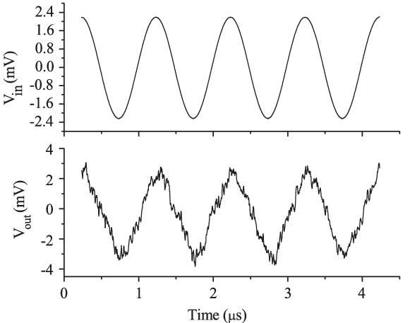
The noise is the random variation of the signal around a mean value (as shown below). Noise is measured by the Root-Mean-Squared (RMS) value of the fluctuations over time. If the signal is measured in voltage, the noise is also represented as voltage.
Signal to noise ratio
The SNR is defined as the ratio of the RMS signal power divided by the RMS noise over the time.
$$\text{SNR}=\cfrac{P_{signal}}{P_{noise}}$$
While designing a system, it is desired to achieve highest SNR possible.
Noise figure
In RF, the most common metric used to quantify the noise added by an individual component or a signal chain is the noise factor (F). It is defined as the ratio of the signal-to-noise ratio (SNR) at the input to the SNR at the output of a circuit block or system. Intuitively, the noise factor represents how much additional noise a component introduces as a signal passes through it.When expressed in decibels, the noise factor is referred to as the noise figure (NF). The noise factor is given by:
$$F=\cfrac{\text{SNR}_{in}}{\text{SNR}_{out}}$$
The noise factor is always larger than or equal to 1, as no circuit can improve the incoming signal's SNR in a real world.
Noise figure is given by:
The noise figure is always larger than or equal to 0 dB.
$$\text{NF}=10\log_{10}{F}$$
SNR improvement by bandwidth reduction
The SNR can be improved through low-pass filtering. Low-pass filtering reduces bandwidth. Noise amplitude is directly proportional to the bandwidth.
$$V_{noise}=\sqrt{4kTR\Delta{}f}$$
While calculating the noise factor, it is assumed that both the signal and the noise occupy the same bandwidth.
Noise figure of a single gain stage
Let us look at a simple model of a noise circuit block as shown in figure below. The input signal Si is accompanied by noise Ni. The gain block has a power gain G1 and adds its own noise Ng1 to the output signal. For simplicity, we assume that the input and output of the gain block are impedance matched to avoid reflections.
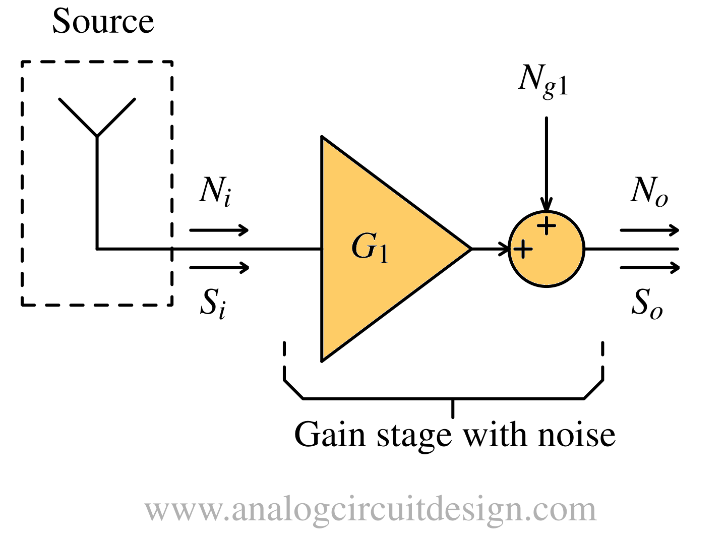
The input signal and noise are both gained by G1, however the noise added by the gain-block is added directly without gain. The output signal and noise powers are then given by :
$$S_o=G_1S_i$$ $$N_o=G_1N_i+N_{g1}$$
The noise factor can be calculated as :
$$F=\cfrac{\text{Input SNR}}{\text{Output SNR}}=\cfrac{S_i/N_i}{S_o/N_o}=\cfrac{S_i/N_i}{G_1S_i/(G_1N_i+N_{g1})}=1+\cfrac{N_{g1}}{G_1N_i}$$
In other words, the noise factor equals one plus the ratio of the noise added by the device under test (DUT) to the amplified input noise. A noiseless block (Ng1 = 0) has a noise factor of F = 1.
Noise figure of cascade of gain blocks
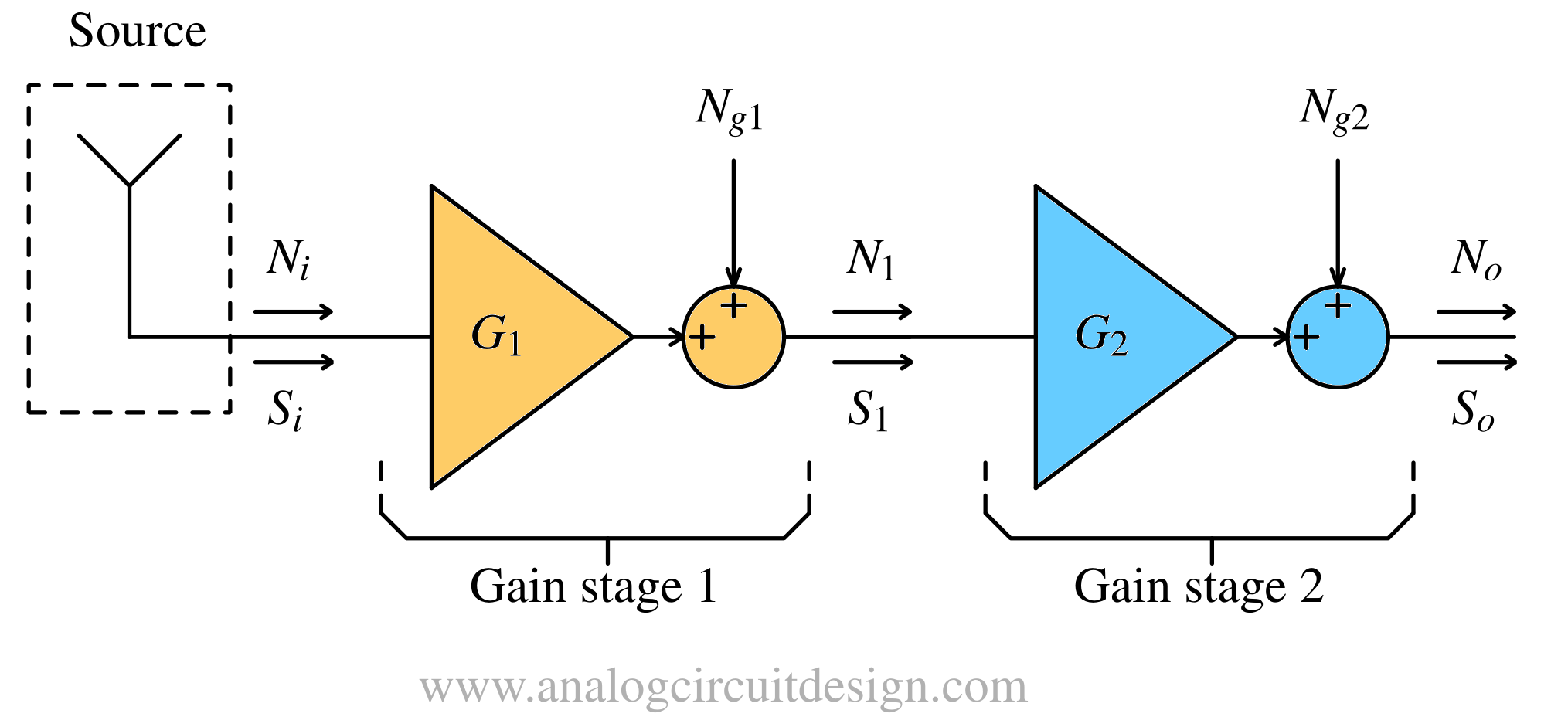
If another gain block is added after the first gain block, the output of first gain block is further amplified. The output of the second gain stage is :
$$S_o=G_2S_1=G_2(G_1S_i)$$ $$N_o=G_2N_1+N_{g2}=G_2(G_1N_i+N_{g1})+N_{g2}=G_2G_1N_i+G_2N_{g1}+N_{g2}$$
Therefore the noise figure is :
$$F=\cfrac{S_i/N_i}{S_o/N_o}=\cfrac{S_i/N_i}{G_2G_1S_i/(G_2G_1N_i+G_2N_{g1}+N_{g2})}=1+G_1\cfrac{N_{g1}}{G_1N_i}+\cfrac{N_{g2}}{G_2G_1N_i}$$
We can extend this formula for N number of gain stages as follows:
$$F=1+\cfrac{N_{g1}}{G_1N_i}+\cfrac{N_{g2}}{G_2G_1N_i}+\cfrac{N_{g3}}{G_3G_2G_1N_i}+\dots{}$$
If we define noise factor for each block as :
$$F_1=1+\cfrac{N_{g1}}{G_1N_i}\implies{}\cfrac{N_{g1}}{N_i}=G_1(F_1-1)$$
$$F_2=1+\cfrac{N_{g2}}{G_2N_i}\implies{}\cfrac{N_{g2}}{N_i}=G_2(F_2-1)$$
$$F_3=1+\cfrac{N_{g3}}{G_3N_i}\implies{}\cfrac{N_{g3}}{N_i}=G_3(F_2-1)$$
$$\vdots$$
$$F_n=1+G_n\cfrac{N_{gn}}{G_nN_i}$$
and substituting it into the noise factor equation, we get :
$$N_F=1+(F_1-1)+\cfrac{F_2-1}{G_1}+\cfrac{F_3-1}{G_1G_2}+\dots{}$$
The above formula is called Friis Formula1. Fi and Gi are the noise factor and power gain of the ith block, respectively.
Some important observations from the Friis formula :
- The overall noise factor Ftotal is always larger than or equal to the noise factor of the first block (F1).
- The noise factor of the first stage is the most critical, since the noise contributions of subsequent stages are attenuated by the gain of all preceding stages. Therefore, it is essential to place the highest gain in the first stage, as this effectively minimizes the noise contribution from subsequent blocks. In LNAs, increasing the gain degrades linearity, so it must be done with care.
- The noise factor of the final stage is divided by the gain of all preceding stages, so its noise contribution is typically insignificant.
Sensitivity
In RF receivers, it is often important to determine the minimum input signal power that can be detected while achieving a specified SNR. This minimum detectable input power is known as the receiver sensitivity. The sensitivity can be calculated as:
$$P_{in,min}=P_n\times{}\text{(min SNR)}\times{}F$$
where Pn is the noise power at the input, SNRmin is the minimum detectable SNR (this requirement comes from the digitizer), and F is the noise factor of the receiver.
The input noise power can be calculated as :
$$P_n=kT\Delta{}f$$
where k is the Boltzmann constant, T is the temperature in Kelvin, and Δf is the bandwidth of the receiver. Dividing Pin,min equation by 1mW and taking 10log10 in both sides of equation to convert the equation into dBm, we get the following formula:
$$10\log_{10}{(P_{in,min})}=10\log_{10}{(kT/1mW)}+10\log_{10}{(\Delta{}f)}+10\log_{10}{F}+10\log_{10}{(\text{Min SNR})}$$
$$P_{in,min}\text{(in dBm)}=-174\,\text{dBm}+10\log_{10}{\Delta{}f}+\text{NF}+10\log_{10}{(\text{Min SNR})}$$
Here, −174 dBm represents the thermal noise power spectral density at room temperature (290 K). From this, it is clear that receiver sensitivity improves with a lower noise figure, a narrower bandwidth, and a smaller required minimum SNR.