Verilog Gate Level Modeling
Gate-level modeling is one of the most detailed ways to represent digital logic in Verilog. It describes circuits explicitly in terms of logic gates and their interconnections, closely resembling actual hardware implementation. Unlike behavioral modeling, which focuses on functionality, gate-level modeling specifies how signals flow through logic gates to produce the desired outputs.
Key Takeaways
- Defines circuits using logic gate primitives
- Allows hierarchical and modular design
- Supports timing control via gate delays
- Provides hardware-accurate representation
Basic Structure of Gate-Level Model
A gate-level module typically consists of:
- Module declaration
- Port definition
- Net declarations (
wire) - Gate instantiations
Example: AND-OR Circuit
module gate_example (input a, b, c, output y);
  wire w1;
  and g1 (w1, a, b);  // w1 = a AND b
  or  g2 (y, w1, c);  // y = w1 OR c
endmodule
y = (a & b) | c using two gate primitives. Gate Instantiation Syntax
General Syntax
gate_type instance_name (output, input1, input2, ...);
Example: 2-Input XOR
xor x1 (y, a, b);
xor→ gate primitivex1→ instance name(y, a, b)→ port connections
You can also omit instance names for simple designs.
Multiple Output Gates
Some primitives can drive multiple outputs using a single input expression.
Example
buf (out1, out2, in1);
not (out3, out4, in2);
Types of Gate Primitives
Verilog provides several built-in gate primitives categorized into logic, buffer, and MOS types.
Logic Gates
| Gate | Description | Example |
|---|---|---|
and | Logical AND | and (y, a, b); |
or | Logical OR | or (y, a, b); |
nand | Negated AND | nand (y, a, b); |
nor | Negated OR | nor (y, a, b); |
xor | Exclusive OR | xor (y, a, b); |
xnor | Exclusive NOR | xnor (y, a, b); |
not | Inverter | not (y, a); |
Buffer Gates
| Gate | Description | Example |
|---|---|---|
buf | Buffer (non-inverting) | buf (y, a); |
not | Inverter (inverting buffer) | not (y, a); |
MOS Primitives (Switch-Level)
| Primitive | Description |
|---|---|
nmos, pmos | Transistor-level connections |
cmos | Complementary MOS switch |
tran | Bidirectional switch |
tranif1 | Conducts when control = 1 |
tranif0 | Conducts when control = 0 |
For most digital design applications, logic and buffer gates are sufficient. Switch level abstraction provides a finer control over circuit however, this level of abstraction is available only in ASIC implementation, not in FPGA designs.
Example Circuits
2-to-1 Multiplexer
module mux2to1 (input a, b, sel, output y);
  wire nsel, w1, w2;

  not  g1 (nsel, sel);
  and  g2 (w1, a, nsel);
  and  g3 (w2, b, sel);
  or   g4 (y, w1, w2);
endmodule
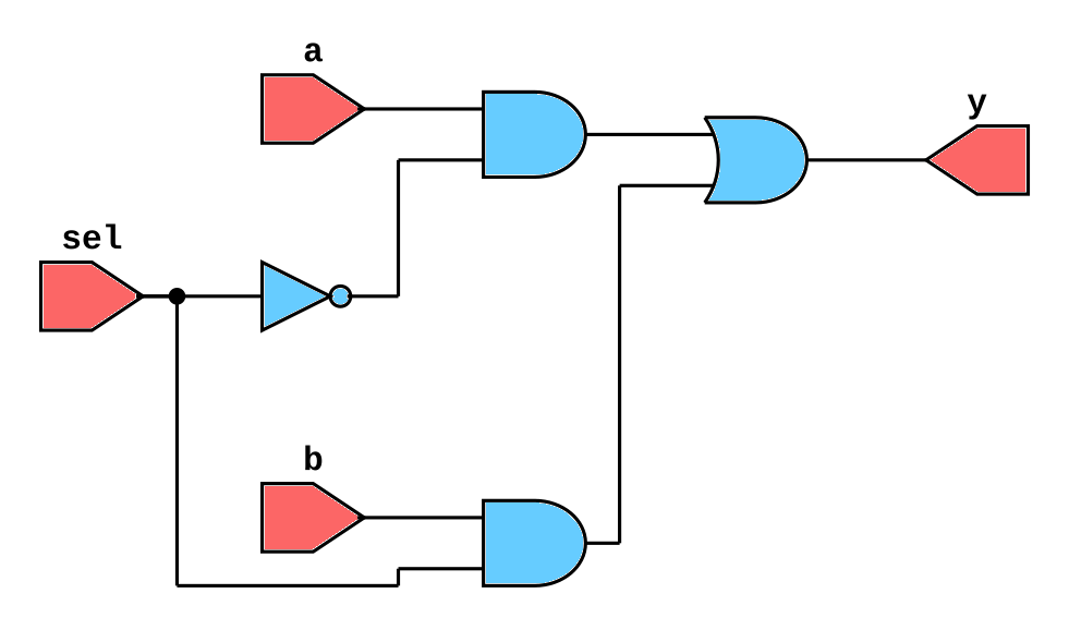
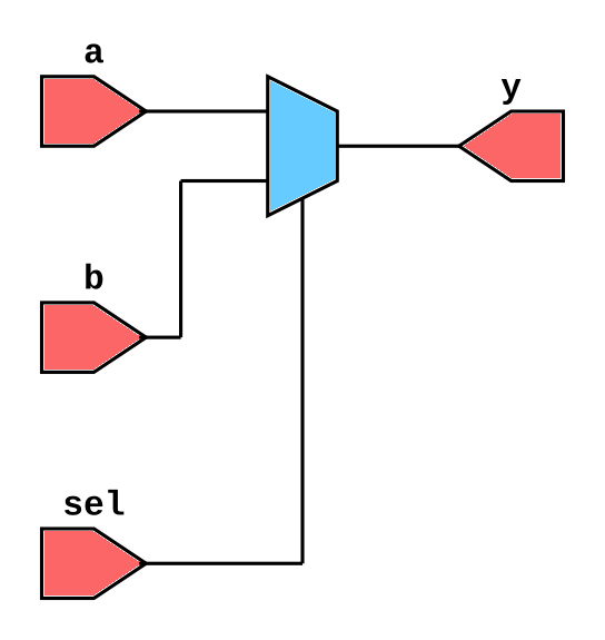
Explanation:
selselects betweenaandb.- Built entirely using primitive gates.
More about Multiplexers : Multiplexers and its applications
Half Adder
module half_adder (input a, b, output sum, carry);
  xor g1 (sum, a, b);
  and g2 (carry, a, b);
endmodule
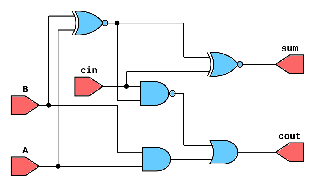
Full Adder
module full_adder_1bit (
    input A,      // 4-bit input A
    input B,      // 4-bit input B
    input cin,         // Carry In
    output sum,   // 4-bit Sum Output
    output cout        // Carry Out
);
  wire s1, c1, c2;
  xor g1 (s1, a, b);
  xor g2 (sum, s1, cin);
  and g3 (c1, a, b);
  and g4 (c2, s1, cin);
  or  g5 (cout, c1, c2);
endmodule
The same full-adder is described below using data-flow modeling. Notice how the number of lines drastically reduced to a single assign statement.
module full_adder_1bit (
    input A,      // 4-bit input A
    input B,      // 4-bit input B
    input cin,         // Carry In
    output sum,   // 4-bit Sum Output
    output cout        // Carry Out
);
    assign {cout, sum} = A + B + cin;
endmodule
Delays in Gate-Level Modeling
Verilog supports modeling of propagation delays directly on gates.
Syntax
and #5 (y, a, b); // 5 time units delay
Example
module delay_example (input a, b, output y);
  and #2 g1 (y, a, b); // Output changes 2 units after inputs
endmodule
Rise, Fall, and Turn-off Delays
You can specify different delays for signal transitions:
and #(2,3) g1 (y, a, b);     // rise=2, fall=3
and #(1,2,3) g2 (y, a, b);   // rise=1, fall=2, turnoff=3
Net Declarations (wire, tri, etc.)
Gate-level connections require nets to link outputs and inputs.
| Type | Description |
|---|---|
wire | Default net type |
tri | Tri-state wire |
supply0, supply1 | Constant 0 or 1 sources |
Example
wire a, b, c;
tri t;
supply1 VDD;
supply0 GND;
Structural Hierarchy
Gate-level modeling allows building hierarchical circuits by instantiating submodules.
Example: Ripple Carry Adder (4-bit)
module full_adder (input a, b, cin, output sum, cout);
  wire s1, c1, c2;
  xor g1 (s1, a, b);
  xor g2 (sum, s1, cin);
  and g3 (c1, a, b);
  and g4 (c2, s1, cin);
  or  g5 (cout, c1, c2);
endmodule

module ripple_adder_4bit (input [3:0] a, b, input cin, output [3:0] sum, output cout);
  wire c1, c2, c3;
  full_adder fa0 (a[0], b[0], cin,  sum[0], c1);
  full_adder fa1 (a[1], b[1], c1,   sum[1], c2);
  full_adder fa2 (a[2], b[2], c2,   sum[2], c3);
  full_adder fa3 (a[3], b[3], c3,   sum[3], cout);
endmodule
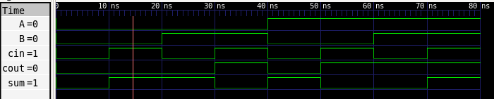
full_adder) is a gate-level sub-block instantiated in a larger design. Gate-Level Testbench Example
module tb_full_adder;
  reg a, b, cin;
  wire sum, cout;

  full_adder uut (a, b, cin, sum, cout);

  initial begin
    $monitor("Time=%0t a=%b b=%b cin=%b sum=%b cout=%b", $time, a, b, cin, sum, cout);
    a=0; b=0; cin=0; #10;
    a=1; b=0; cin=0; #10;
    a=0; b=1; cin=1; #10;
    a=1; b=1; cin=1; #10;
    $finish;
  end
endmodule
Advantages of Gate-Level Modeling
- Accurate hardware representation — Closest to actual logic implementation
- Useful for timing analysis — Delays and gate counts can be simulated
- Easy verification of synthesis output — Matches netlist from synthesis tools
- Hierarchical structure — Supports modular and reusable designs
Limitations
- Complex for large systems — Writing large designs at gate-level is tedious
- Poor readability — Difficult to debug or modify
- Time-consuming simulation — Each gate adds event simulation overhead
- Not ideal for early functional design — Behavioral/RTL preferred initially
When to Use Gate-Level Modeling
Use gate-level modeling when:
- You need fine-level control of logic connections.
- You need an even more optimized digital circuit block, which could be better than synthesis.
- Designing small combinational or sequential blocks for educational or verification purposes.
Summary
Gate-level modeling provides an explicit hardware-level description using built-in primitives like and, or, not, and xor. While it’s not commonly used for complex designs today, it remains fundamental for learning digital design principles and verifying synthesis results.