555 Timer IC
The 555 timer integrated circuit, introduced in 1972 by Signetics, is a timing generation IC which is popular for its simplicity, affordability, and versatility. It is found in countless applications and is commonly configured as an oscillator. Other applications are pulse generator, frequency divider, PWM generator, etc. Derivatives like the 556 and 558 combine multiple timers in one package.
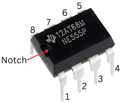
555 timer IC pinout
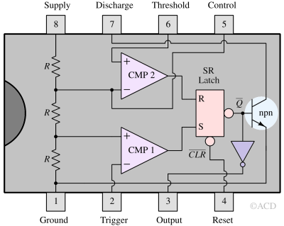
| Pin Number | Pin Name | Function |
|---|---|---|
| 1 | Ground (GND) | This pin is connected to the circuit ground |
| 2 | Trigger (TRIG) | A voltage less than (⅓)VCC in this pin sets the internal SR latch. The output (Pin 3) becomes logic HIGH. The output will remain until a voltage higher than (⅔)VCC is applied at pin 6 (Threshold). |
| 3 | Output (OUT) | In the low output state, the voltage will be nearly 0.1V (legroom). In the high output state, the voltage will be near 1.7V (headroom) below the supply voltage. With an increase in output current, the headroom and legroom voltages worsen. The output can source or sink up to 200 mA. |
| 4 | Reset (RST) | A low voltage applied to this pin will reset the internal SR latch and cause the OUTPUT (pin 3) to go low. This pin overrides the other two inputs (i.e., S and R) of the SR latch. When not used, this input should remain connected to SUP (Pin 8). |
| 5 | Control voltage (CTRL) | The internal threshold voltage of ⅔ VCC can be changed using this pin. This pin can be used to change the pulse width of the output. When not in use, this pin should be connected to the circuit ground via a 0.01uF capacitor to filter noise, which can trigger the internal comparator. |
| 6 | Threshold (THR) | Usually, the timing capacitor (CT) is connected to this node to monitor the rise and fall voltage. The other terminal of the capacitor is connected to the ground. In Bistable mode, it is connected to the ground. |
| 7 | Discharge (DIS) | This is the pin through which the RC circuit is discharged to the ground when the threshold voltage hits ⅔ VCC mark. |
| 8 | Supply (SUP) | This is the positive power supply pin and can take a voltage between 5 and 15 V |
555 timer IC internal circuit diagram
The timer 555 IC is made up of the following building blocks:
Internal threshold-generator and voltage-divider
It is the simplest to understand. Three equal resistors (R1, R2, R3) are connected from VCC (Pin 8) to GND (Pin 1). Each resistor is 5kΩ for BJT-based ICs. These are 100kΩ each for CMOS-based ICs. These resistors are the significant source of quiescent current consumption in BJT-based timer 555 ICs. Using a 100kΩ resistor in BJT-based timers causes substantial errors in threshold generation because of base currents (IB). If seen carefully, the CMOS-based timers (LMC555, TLC551, TS555) consume only 130uA, while BJT timers (NE555) consume 3mA of power. This low power consumption makes CMOS ICs ideal for portable battery-operated applications.
The CONTROL pin can change these threshold voltages (Pin 5). If the CONTROL pin is left open, the thresholds are set to ⅔ VCC and ⅓ VCC. If a voltage VCTRL is forced in the CONTROL pin, the thresholds are set to VCTRL and ½ VCTRL.
Trigger comparator (CMP 1)
The comparator's non-inverting (+ve) input terminal is connected to the voltage divider's lower reference voltage (⅓ VCC), and the inverting (-ve) input terminal is connected to TRIGGER (pin 2). The output of this comparator is connected to the set terminal of the internal SR latch. If the voltage at the TRIGGER pin is lower than ⅓ VCC or ½ VCTRL, it produces logic high, setting the SR latch. Setting the SR latch means the output of SR is one, irrespective of its previous value.
Threshold comparator (CMP 2)
The comparator's inverting input terminal is connected to the voltage divider's upper reference voltage (⅔ VCC), and the comparator's non-inverting input terminal is connected to THRESHOLD. The output of this comparator is connected to the reset terminal of the internal SR latch. If the voltage at the THRESHOLD pin is higher than ⅔ VCC or CONTROL pin, it produces logic high, resetting the SR latch. Resetting the SR means the output of SR is zero, irrespective of its previous value. 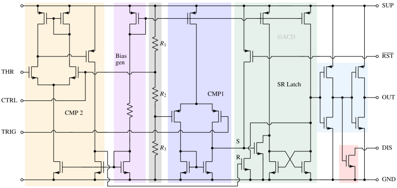
SR latch
A set-reset latch stores the timer's state and is controlled by the two comparators (CMP1 and CMP2). RESET (Pin 4) overrides the other two inputs (i.e., S and R). Thus, the latch (and, therefore, the entire timer) can be reset anytime using the RESET pin.
Discharge NPN
This is an open-collector NPN whose base is connected to the output of the SR latch. The collector is connected to the DISCHARGE pin, and the emitter is connected to the GND pin. When the SR latch is in reset mode, the NPN base is pulled high, pulling down the DISCHARGE pin to the ground.
555 timer IC circuits
Some very common circuits of 555 timer IC are mentioned below :
Astable multivibrator
This mode is also called an astable timer circuit. It is the most common use of a 555-timer IC circuit. In an astable circuit, the output voltage continuously alternates between VSUP (HIGH) and 0 (LOW) volts. This is called astable mode because the output is unstable in both HIGH and LOW states. If it goes HIGH, it will come to LOW soon and vice-versa. This makes astable mode ideal for applications that require a continuous square wave output, such as clock pulse generation, tone generation, or other timing functions.
Circuit connections astable multivibrator mode
The key external components required are R1, R2, CT, and a 10nF capacitor. These components will decide the frequency and duty cycle of the output waveform. For simplicity, we will use the internal thresholds (i.e., ⅓ VCC and ⅔ VCC) and keep the CONTROL pin floating with a 10nF capacitor connected to the ground. The junction of R2 and CT is connected to the THRESHOLD (pin 6) and TRIGGER (pin 2) pins to monitor the capacitor voltage. Both pins are comparator inputs. The junction of R1 and R2 is connected to the DISCHARGE (pin 7). The RESET (pin 4) is permanently tied to VCC to avoid undesirable reset. SUPPLY (pin 8) is connected to VCC, and pin 1 is connected to the ground. 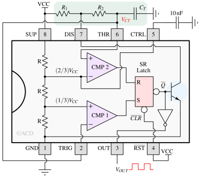
Working in astable multivibrator mode
Step-by-step working of a 555 timer in astable multivibrator mode is mentioned below :
- In the startup phase, the capacitor starts charging from 0V. The output of comparator-1 is high, and the output of comparator-2 is low, setting the SR latch (S=1, R=0), which disables the discharge NPN. So, the capacitor (CT) charging continues.
- Soon, the capacitor voltage crosses ⅓ VCC, which makes the output of comparator-1 low. However, the SR latch retains the state (S=0, R=0, and Q=1) and allows the capacitor to charge. The charging path is R1, R2, and CT, so the charging time constant is (R1+R2)CT. The output (pin 3) is logic HIGH.
- After some time, the capacitor voltage reaches ⅔ VCC, producing a logic high at the output of comparator-2, resetting the SR latch (S=0, R=1). This leads to NPN pulling the DISCHARGE pin to the ground.
- The capacitor has started discharging, and its voltage has begun falling. The discharge path is R2 and CT, so the time constant is R2CT. The output of comparator-2 has gone back to zero again. The SR latch will retain the state (S=0, R=0, and Q=0). The output (pin 3) is logic LOW.
- The capacitor's discharge will continue until the voltage goes below ⅓ VCC. After that, the output of comparator-1 will go high, setting the SR latch (S=1, R=0). This will disable the discharge NPN, allowing the capacitor to be charged again. Now, the cycle repeats from step 2 again.
If we ignore the startup phase, we can easily calculate the output waveform's ton and toff times. Carefully observing the charge/discharge path, we can note that during ton, the time constant is (R1+R2)CT, while for toff, the time constant is R2CT. Ton: $$v(t)=\text{VCC}+\left(\cfrac{1}{3}\text{VCC}-\text{VCC}\right)\exp{\left(-\cfrac{t}{(R_1+R_2)C_T}\right)}$$ $$v(t_{on})=\cfrac{2}{3}\text{VCC}$$ $$\implies{}\cfrac{2}{3}\text{VCC}=\text{VCC}+\left(\cfrac{1}{3}\text{VCC}-\text{VCC}\right)\exp{\left(-\cfrac{t_{on}}{(R_1+R_2)C_T}\right)}$$ $$\implies{}t_{on}=\ln(2)(R_1+R_2)C_T=0.693(R_1+R_2)C_T$$ Toff: $$v(t)=0+\left(\cfrac{2}{3}\text{VCC}-0\right)\exp{\left(-\cfrac{t}{R_2C_T}\right)}$$ $$v(t_{off})=\cfrac{1}{3}\text{VCC}$$ $$\implies{}\cfrac{1}{3}\text{VCC}=0+\left(\cfrac{2}{3}\text{VCC}-0\right)\exp{\left(-\cfrac{t_{off}}{R_2C_T}\right)}$$ $$\implies{}t_{off}=\ln(2)R_2C_T=0.693R_2C_T$$ Frequency: $$F=\cfrac{1}{0.693(R_1+2R_2)C_T}$$ Duty Cycle(D): $$D=\cfrac{R_1+R_2}{R_1+2R_2}$$ The duration for which the output is zero is called “space,” while the duration for which the output is high is called “mark.” The duty cycle in this astable multivibrator mode is not 50%.
Bistable (Flip-flop circuit) mode
In the bistable mode, only the internal SR latch is used, and no external RC circuits are involved. It is called bistable because the output is stable in both the HIGH and LOW states. The output changes only when there is an external interrupt. For example, a HIGH output will go LOW once it receives an interrupt and stay LOW until the next interrupt is provided.
Circuit connections in bistable mode
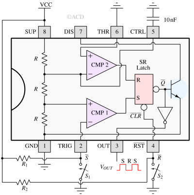
The key external components required are a 10nF capacitor, R1 and R2 (as pullup resistors), and two switches (S1 and S2). The 10nF capacitor will be connected to the CONTROL pin. The DISCHARGE pin is left open since no RC circuit is discharging. SUPPLY (pin 8) is connected to VCC, and pin 1 is connected to the ground. THRESHOLD is connected to GND.
Working of Timer 555 in bistable mode
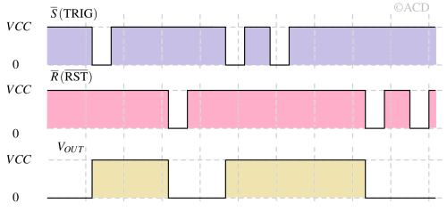 Let’s note some observations. The THRESHOLD is permanently tied to GND, meaning the output of CMP 2 is always low. This means the R input of the internal S R latch is zero. Therefore, we cannot reset the latch using R input. However, we can use the CLR, which comes out as an RST pin, to reset the SR latch. The pins TRIGGER and RESET are named S and R because they reach the SR latch through an inverting stage. If TRIGGER is pulled low using the switch, the output of the CMP 1 becomes HIGH, setting the SR latch and causing the VOUT to go HIGH. TRIGGER does not affect the VOUT when it pulls to VCC again, as the SR latch is in retain mode. If RST goes low, the internal SR latch clears, and VOUT goes LOW. The VOUT retains its low state even if the RST returns to HIGH.
Monostable multivibrator
Monostable multivibrators have only a single stable state (hence the name "mono") and generate a single output pulse when triggered externally. They return to their initial (stable) state after a period decided by the RC circuit's time constant. For example, 555 timers' stable state is LOW. The VOUT remains LOW when there is no input. When an input is applied, the VOUT goes to HIGH, stays there for a time “TON,” and returns to the LOW state after TON time.
Circuit connections in monostable mode
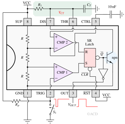 The external components required are a resistor R1, capacitor CT, a 10nF capacitor, resistor Rp, and one switch (S1). The 10nF capacitor will be connected to the CONTROL (pin 5). The DISCHARGE (pin 7) and the THRESHOLD (pin 6) are connected to the junction of R1 and CT. SUPPLY (pin 8) is connected to VCC, and GND (pin 1) is connected to the ground. The TRIGGER (pin 2) is pulled up using resistor Rp, and a switch is connected to the ground to provide a signal. RESET (pin 4) is connected to VCC.
Working of 555 timer IC in monostable multivibrator mode
In Monostable mode, VOUT responds only when the TRIGGER is pulled low. The TRIGGER can return to its original state without affecting VOUT, as shown in the figure. The time duration for which VOUT is high is denoted by Ton. Multiple TRIGGER pulses can come now, but they will not affect VOUT. Having different TRIGGER pulse widths does not impact VOUT. 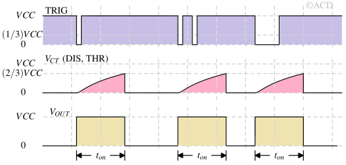
The initial state of TRIGGER is HIGH because it is pulled high using RP. The output of CMP-1 is LOW. We do not know the initial state of the VCT node. VCT node is the junction of the external R1 resistor and CT capacitor. Let’s assume it is HIGH, which means the output of CMP 2 is HIGH. So, the SR latch is reset, causing the discharge of the VCT node to zero. When the VCT node is at zero, CMP-2’s output is zero. Note that CMP-1’s output is also zero. This means the SR latch is in retain mode. So, we observe that VCT HIGH is not stable; it will return to a LOW state. Also, we observe that Q=0 because the reset was engaged. So, VOUT being LOW is the stable state. When TRIGGER is pulled down below ⅓ VCC, the output of CMP-1 goes high, setting the SR latch; this disables the discharge NPN and allows the CT to charge through R1. As soon as the VCT reaches ⅔ VCC, this resets the SR latch, and the VOUT becomes LOW. This also activates the discharge NPN, pulling the VCT node to zero.
50% Duty cycle mode
The astable multivibrator circuit does not produce a symmetric 50% duty cycle signal. This is because the charging and discharging paths see different resistances. The capacitor CT sees R1+R2 while charging and only R2 while discharging. To create a 50% duty cycle output waveform, we must ensure that the charging and discharging paths have similar resistance values.
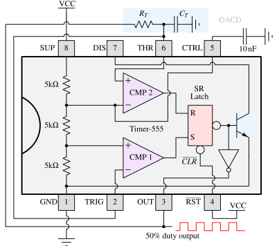
$$T_{on}=T_{off}=\ln(2)R_TC_T$$
Duty cycle (D) :
$$\text{D}=50%$$
Frequency (F) :
$$\text{F}=\cfrac{1}{2\ln(2)R_TC_T}$$
PWM generation mode
The 555 timers can be configured to generate a PWM signal, which can be used to control the brightness of the LED, the speed of DC motors, the position of servo motors, etc. The astable multivibrator circuit can be modified to create a PWM signal. A variable resistor (VR1) must be inserted at the junction of R1 and R2 to vary the duty cycle manually. It is discussed in detail in: PWM using 555 timer IC
555 Timer IC specifications
| Sr. No. | Property | BJT based IC | CMOS based IC |
|---|---|---|---|
| 1 | Maximum supported Frequency | 500kHz | 3MHz |
| Supply voltage | 4.5V - 15V | 1.5V - 12V | |
| 2 | Quiescent current | 10mA at 15V supply | 0.2mA at 12V |
| 3 | Output Voltage Drop (High) | 1.5V (at 50mA ILoad) | 0.7V (at 10mA ILoad |
| 4 | Output Voltage Drop (Low) | 0.7V at 50mA ILoad | 1V at 50mA ILoad |
| 5 | OUTPUT current capability | ~200mA | ~50mA |
| 6 | Discharge NPN's current capability | 10mA for VLOW = 100mV | 10mA for VLOW = 150mV |
| 7 | IC examples | NE555, NE556, NE558, LM555 | LMC555, TS555 |
555 timer IC applications
555 timer finds many applications due to its versatility. Some applications are mentioned below:
The 555 timer is a versatile IC (integrated circuit) that can function in various modes and applications, making it a popular choice for hobbyists, engineers, and designers. Here are some typical applications of the 555 timer:
- The Astable Multivibrator (Oscillator) mode: This mode of 555 timer IC can be used in LED flashers, clock pulses for digital circuits, and other applications. It is the most common application of the 555 timer IC.
- A Monostable Multivibrator (One-shot Pulse Generator): This mode can be used for timed delay circuits, debounce switches, and frequency dividers.
- Bistable Multivibrators (Flip-Flops): This mode of 555 timers can be used as latching relays, simple memory elements, and BOM consolidation devices.
- PWM (Pulse Width Modulation) Generator: With some modification in astable multivibrator mode, a 555 timer IC can vary the duty cycle, which can be used for Motor speed control, light dimming, servo-motor control, etc.
- Tone Generation: The 555 timer can produce audio tones at different frequencies by configuring it in astable mode. The output wave must be filtered using a bandpass filter tuned at oscillation frequency to get a clean sinusoid. Typical applications include sound effects, sirens, alarm circuits, and metronomes.
- Time Delay Circuit: The 555 timer IC's monostable mode is frequently used to create delay circuits in which the output is delayed after the trigger input. Typical applications are debouncing switches, automatic shut-offs, and delay circuits for cameras or relays.
- Frequency Divider: The 555 timer can divide a higher-frequency signal into lower-frequency pulses, serving as a frequency divider. This can be done by using the monostable mode of the 555 timer. For example, if a frequency division of 5 is needed, the Ton can be set to 5 times the incoming time period.
- Voltage-controlled oscillator: With some modifications, the 555 timer IC can act as a voltage-controlled oscillator (VCO), changing frequency in response to a varying control (pin 5) voltage. This mode can be used in Frequency modulation circuits, analog synthesizers, and radio transmitters.
- Pulse Generator: It can be configured to generate single pulses or pulse trains, making it ideal for test and measurement applications. It is typically used in signal testing, triggering other circuits, and digital circuit debugging.