Analog circuits interactive design tools & resources
Your online easy to use design companion
×


Recent Articles
Control
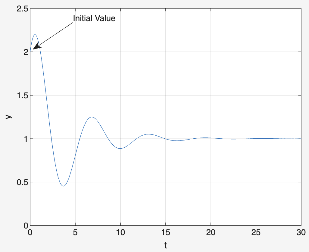
Initial Value Theorem: Predicting Initial System Behavior from the Laplace Domain
The initial value theorem relates the behavior of a function as time approaches zero to its Laplace transform, helping analyze system response at the start.

Data-Converters
R-2R Ladder DAC: Working Principle, Advantages and Limitations
An R-2R ladder DAC converts digital binary inputs into a corresponding analog voltage using a network of resistors arranged in a repeating R and 2R pattern.
Tools
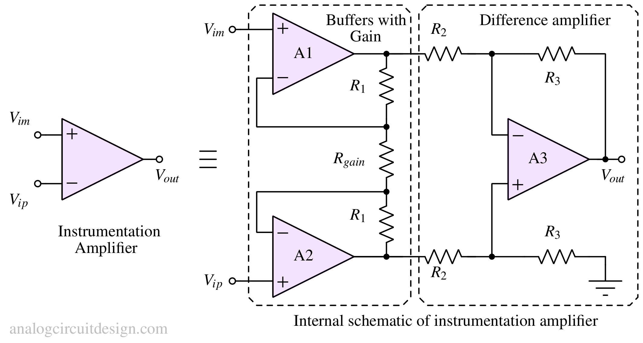
Instrumentation Amplifier Calculator: Gain, Resistor Values Calculation Tool
An instrumentation amplifier calculator computes the output voltage and overall gain based on resistor values and input voltages in a three-op-amp configuration.