Introduction
A Class D amplifier, is a switching amplifier where the active devices, typically MOSFET transistors function as on/off switches rather than operating in their linear gain region as in conventional amplifiers. They are also called power amplifiers since they deliver significantly more power to the load than the source. They have the best power efficiency among classes of amplifiers.
Working principle
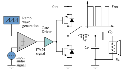
The operation of a Class D amplifier relies on high-speed switching and filtering rather than traditional linear amplification. The analog input signal is first converted into a high frequency Pulse Width Modulation (PWM) output, where the pulse width is proportional to instantaneous amplitude of the audio signal. This PWM signal controls the output transistors (typically power MOSFETs), which alternate between fully on and fully off states. Because the devices conduct with negligible resistance when on and carry no current when off, power loss is extremely low. This results in very high efficiency. The amplifier’s raw output is a PWM waveform rather than a direct analog signal. An LC low-pass filter at the output stage removes the fast rise/fall edges, leaving behind the reconstructed audio waveform to drive the loudspeaker.
Open loop class D amplifier
An open-loop Class D amplifier is a basic type of Class D (switching) amplifier that operates without any global feedback loop from the output back to the input. It relies strictly on the accuracy of its modulation and switching stages to track the input signal, with no error correction or compensation for non-idealities, power supply noise, or device nonlinearities. It is very simple to implement.

Closed loop class D amplifier
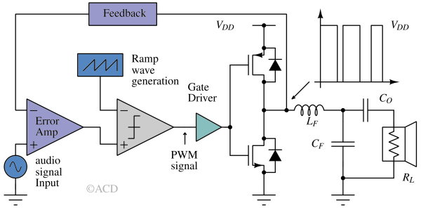
Many Class D amplifiers employ negative feedback from the PWM output back to the input. This closed-loop design improves linearity and significantly enhances the power supply rejection ratio (PSRR). In contrast, open-loop Class D amplifiers lack feedback and inherently exhibit 0 dB PSRR.

Deploying negative feedback bring noise shaping in Class D amplifiers. This effectively suppresses in-band noise caused by the nonlinearities of the pulse-width modulator, output stage, and variations in supply voltage. This approach is conceptually similar to the noise-shaping techniques employed in sigma-delta modulators.

Class AB vs Class D amplifier
The primary and main difference between linear and Class D amplifiers is the efficiency. Practical efficiency is 50% (maximum efficiency 78%) for class AB amplifiers. Practical efficiency of class D amplifiers could easily reach 90%. Unlike Class AB amplifiers with high PSRR, Class D amplifiers have 0 dB PSRR and rely on negative feedback to counter supply voltage variations.
| Class | Method | Sound Quality | Efficiency |
|---|---|---|---|
| Class A | Linear | Best | Lowest |
| Class B | Linear | Not good | Better |
| Class AB | Linear | Good | Between A & B |
| Class D | Switched (PWM) | Good | Best |
Conduction angle in class D amplifier
Concept of conduction angle does not apply in class D amplifier, because it is a switching topology. Conduction angle applies on linear power amplifier topologies. Class D amplifiers can be related to class B amplifiers where only one transistor turn on at a time.
Output impedance
In a Class D amplifier, the output stage uses high-speed switches that connect the load alternately to the supply rails through a PWM signal. This PWM is then low-pass filtered to reproduce the desired analog signal for the speaker. Unlike linear amplifiers (Class A, B, AB, C), where output impedance can be derived from a small-signal model around an operating point, the switching nature of Class D makes impedance analysis less straightforward. While a linearized model can be created, it is more complex and requires additional effort.
One method to find the output impedance of switching amplifier is mentioned here – https://www.cppsim.com/Publications/Theses/kuo_mthesis.pdf
Inductor
Value of inductor is based on the switching frequency. Higher switching frequencies allow smaller inductors.
Following points should be taken care of while selecting a inductor for class D amplifier:
- Lower DCR reduces power loss and heat dissipation. Choose inductors with low winding resistance to maximise amplifier efficiency.
- The inductor core must support the maximum expected current without saturating. Saturation causes a sudden drop in inductance, degrading filter performance and causing distortion. Ensure the saturation current rating is above the maximum output current of the amplifier. Ferrite cores are common.
- Toroidal inductors are better for better EMI performance.
- Skin effect at higher frequencies.
- Temperature rise with average DC current flowing through the inductor.
Power calculation
Audio power amplifier design typically uses speakers with impedances from 3 Ω to 32 Ω. The output voltage (VO) is specified as an RMS value and the following equation is used:
$$P_{load}=\cfrac{V_{o,rms}^2}{R_{load}}$$
$$V_{o,rms}=\cfrac{V_{o,p}}{\sqrt{2}}=\cfrac{V_{o,pp}}{2\sqrt{2}}$$
$$V_{o,p}=\text{Peak Voltage}$$
$$V_{o,pp}=\text{Peak to Peak Voltage}$$
Gate Driver and Dead Time
There are two challenges with power MOSFETs in class D amplifiers:
- Power MOSFETs are typically large devices, which results in substantial gate and drain capacitances (ranging from ~100 pF to 2 nF). To switch these gates on and off within just a few nanoseconds, the driver must supply a high charging and discharging current (high CdV/dt capability).
- It is critical that the top and bottom MOSFETs never turn on simultaneously. If both conduct at the same time, a large shoot-through (or crowbar) current flows directly from the supply to ground (e.g., VDD/Rsw = 5V/1Ω = 5A). This not only increases power loss and reduces efficiency but can also cause the power supply to trip. To prevent this, the gate signals are carefully timed so that one MOSFET turns off before the other turns on. The intentional delay between these events is known as dead time, during which both transistors remain off.
So, the job of a Gate driver is to transient source and sink currents, facilitate precise dead-time control as well as isolate control signals from high-voltage, support high-side and low-side transistor driving etc.
References
- Click and Pop Noise – https://www.ti.com/lit/an/slea044/slea044.pdf
