Bandgap voltage reference
Bandgap voltage reference is a temperature independent voltage reference used for generating a constant voltage across temperatures and supply voltages. In classic bandgap references, the voltage equals the extrapolated bandgap of intrinsic silicon, i.e., 1.2V.
It is one of the most essential circuits to have in an integrated circuit. Almost every integrated circuit has at least one bandgap circuit.
Principle of operation of bandgap reference
Almost every circuit element reacts with temperature. So, keeping the current/voltage across them constant without external voltage reference is challenging.
BJTs have known temperature-dependent behavior, which is fairly similar in every process/technology. Usually, with BJTs, we can generate both positive slope (PTAT) and negative slope (CTAT) voltages. If we make both slopes' magnitude equal and add the PTAT and CTAT voltages to cancel the slopes, we can get a voltage with zero slope/constant voltage (ZTAT) with temperature.
CTAT voltage
If we connect an ideal current source in a diode-connected BJT, the VBE will decrease with an increase in temperature. This behavior is called Complementary to Absolute Temperature (CTAT).
$$V_{BE}=\cfrac{kT}{q}ln{\left(\cfrac{I_c}{I_s}\right)}$$
Ic is the collector current. Is is the reverse saturation current; it depends strongly on temperature, device construction, area, and doping levels. T is the absolute temperature, k is the Boltzmann constant, and q is the charge.
It may look like VBE increases with temperature, but the Is term inside the natural log also increases with higher-order dependence on temperature.
PTAT voltage
Let's take the difference of VBE of two BJTs having different current densities (same current but different emitter areas). The difference in VBE happens to increase with an increase in temperature. This increase in voltage with increase in temperature is called Proportional to Absolute Temperature (PTAT).
ZTAT voltage
A bandgap reference voltage is called Zero to Absolute Temperature (ZTAT). This means that the slope of voltage with temperature is zero. Which also means that the voltage is constant with temperature.
Classic bandgap voltage references
Classic bandgap reference circuits are commonly used in electronic devices to provide a stable and precise voltage reference, often at a fixed voltage of 1.2V or 1.25V. These circuits are designed to maintain their output voltage across various temperature and power supply fluctuations.
Widlar bandgap reference

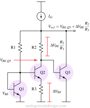
A loop is formed by the VBE of Q1 and Q2 and resistor R3. Consequently, the voltage drop across R3 is ΔVBE of Q1 and Q2. For the fact of ΔVBE to be truly PTAT without nonlinearity, the currents through Q1 and Q2 must be equal or at least very similar. If we see the circuit, it is fair the assume that VBE, Q1 is almost similar to VBE, Q3 which means the voltage drop across R1 and R2 is similar. This makes current through Q1 and Q2 also similar. The PTAT current through R3 flows through R2 and creates a voltage drop of ΔVBER2/R3. The overall voltage at the output is the sum of VBE,Q3 and R2's voltage drop :
$$V_{ref}=V_{BE,Q3}+\Delta{}V_{BE}\cfrac{R_2}{R_3}$$
More about Widlar voltage reference can be found in this paper: New developments in IC voltage regulators
Brokaw bandgap reference
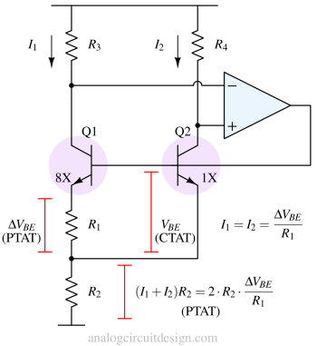
The Brokaw bandgap reference is a commonly utilized voltage reference circuit in integrated circuits, delivering an output voltage typically set at around 1.25V while exhibiting minimal sensitivity to temperature variations. This specific circuit is categorized as a type of bandgap voltage reference, named in honor of its creator, Paul Brokaw.

Within the Brokaw bandgap reference, the circuit employs negative feedback, facilitated by an operational amplifier, to maintain a consistent current flow through two bipolar transistors possessing distinct emitter areas. The principle is similar to other bandgap reference circuits. The transistor with the greater emitter area (Q1) necessitates a lower base-emitter voltage to achieve an equivalent current. The difference between the two base-emitter voltages (VBE,Q2 - VBE,Q1) exhibits a positive temperature coefficient (PTAT), meaning it rises with increasing temperature. In contrast, the base-emitter voltage of each transistor exhibits a negative temperature coefficient (CTAT), decreasing as the temperature increases.
PNP bandgap reference
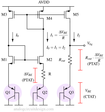
This bandgap is compatible with standard CMOS technology because it uses PNP instead of NPN. Therefore, the cross-section of PMOS can form the PNP in this bandgap. This circuit is used when a process flow supports only PNP.

Sub 1-V bandgap voltage reference
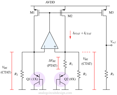
Most of the bandgap we have seen now can capable of generating a voltage of 1.25V. However, in some low-voltage applications, a sub-1V bandgap reference is required. This paper by Banba describes a nice way to achieve sub-1V bandgap reference.

The sub-1-V bandgap adds both PTAT and CTAT information using current. It deploys an operational amplifier to add both the PTAT and CTAT current. That current is now ZTAT, which is dropped across a resistor R3 to get the desired sub-1V output.
Sources of error in bandgap reference
The transistor's non-idealities cause the bandgap reference to change slightly change with temperature which may not be accepted in some applications. Following are some sources of error in a bandgap reference :
Base currents of BJTs
Base currents of BJTs create extra voltage drop across the resistor where the base is not connected to very low impedance nodes. Examples of low-impedance nodes are ground, the output of an operational amplifier, etc.
Curvature of VBE
If we take a detailed look into VBE,
$$I_C=C\cdot{}T^n\cdot{}\exp{\left(\cfrac{\left(V_{BE}-V_{bg}\right)}{kT/q}\right)}$$
Where C is a proportionality constant, Vbg is the extrapolated bandgap voltage at 0K, and n is a constant depending on the doping profile. IC also has some temperature dependence (usually m = 1), as we saw in the PNP bandgap reference and Brokaw bandgap reference. Let's assume,
$$I_C=B\cdot{}T^m$$
If we expand the expression for VBE near reference temperature (Tr),
$$V_{BE}(T)=V_{bg}\left(1-\cfrac{T}{T_r}\right)+\cfrac{T}{T_r}V_{BE}(T_r)-(n-m)\cfrac{kT}{q}ln{\left(\cfrac{T}{T_r}\right)}$$
The third term in the above expression is a nonlinear term, which gives the curvature. For high-precision applications across temperatures, the curvature itself can be a problem.
To read more about curvature correction, visit this page: Curvature correction in Bandgap.
Finite output impedance and mismatch of transistors
The finite output impedance of the transistor causes a current mismatch in current mirrors. Also, the mismatch between two transistors also causes a current mismatch. This leads to a temperature-dependent offset in the bandgap reference.
Startup circuit
Most of the bandgap circuits are self-biased circuits. Self-biased circuits mean that the current required to bias the circuit elements depends on the correct operating point of the same circuit. Such circuits have two possible operating points.
- One is zero currents through every branch.
- Another is the desired current through every branch.
So, we require a circuit that ensures the zero current condition is not a solution. The only solution is the desired operating point. This circuit is called a startup circuit. Once the circuit comes to the desired operating point, the startup circuit turns off.