Boost (Step-Up) converter
A boost converter is a DC-DC (direct current to direct current) converter used to step up or increase a DC voltage from a lower to a higher level. It is also called a step-up converter. It converts a lower DC voltage input to a higher DC voltage output using an inductor, a switch (typically a transistor), a diode, and a capacitor.
Boost converter analysis online design tool

Boost converter circuit diagram

The fundamental configuration of a boost converter comprises following elements:
- Inductor (L): Playing a crucial role, the inductor stores and releases energy throughout switching cycles. Its primary function involves maintaining energy storage during conversion while regulating current flow.
- Switch (Q1): Acting as a key component, the switch—typically a MOSFET or IGBT—manages energy transfer by intermittently connecting and disconnecting the inductor to the load. This control mechanism is fundamental in governing the input-to-output energy flow. The gate of this switch is controlled by an IC (e.g., MC34063)
- Diode (D): During switch-off intervals, the diode facilitates unidirectional current flow in the circuit, directing it towards the output. When the switch is open, it prevents current from reverting to the input side.
- Output capacitor (C): Responsible for stabilizing and smoothing the voltage across the load, the output capacitor ensures a steady output voltage. It also filters high-frequency voltage ripples, contributing to consistent output for the load.
- Load resistor (R): Symbolizing the electrical load connected to and powered by the boost converter, the load resistor (R) represents the requirement for the converter to supply the necessary voltage and current to sustain the load's operation.
Operating principle of boost converter
The basic operation of a boost converter involves two main states: switch is ON and switch is OFF
Switch is ON

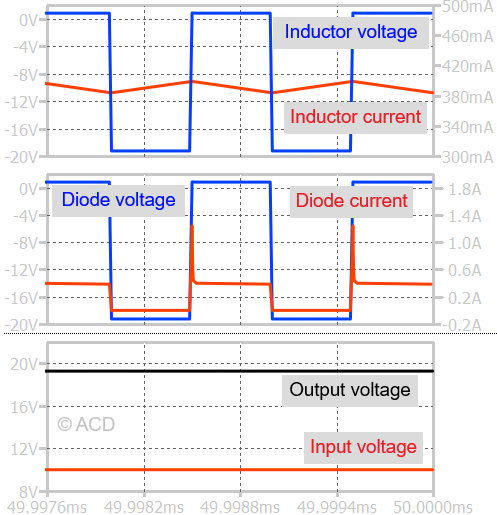
During the ON state, a logic high is applied to the gate of the switch (N-channel MOSFET). The input voltage is applied to the inductor, causing current to flow through it and storing energy in its magnetic field. The diode's anode is shorted to ground, and the cathode is still at the output voltage. So, the diode is turned off. This means there is no energy supply to the output capacitor. The output capacitor solely provides the load current.
Until the time interval, Ton, the inductor current rises linearly because a constant voltage is applied. The change in inductor current can be written as:
$$\Delta{}I_L(on)=\cfrac{V_{in}}{L}T_{on}$$
Switch is OFF

When the switch is opened (OFF state), the inductor continues to have the current flowing in the same direction. It turns on the diode by increasing the voltage at the anode of the diode. The charges will accumulate at the anode if the diode does not turn ON. The diode turns ON and allows the current to flow through the load and the capacitor. This charges the capacitor as well so that it has enough energy for the next turn-off cycle.
Since the voltage across the inductor has flipped direction, the current through it will linearly reduce for the time duration Toff. The change in current can be represented as :
$$\Delta{}I_L(off)=\cfrac{V_{in}-V_{out}}{L}T_{off}$$
In the above equation, Vout is greater than Vin. So, the current is decreasing, and ΔIL is negative.
Boost equation and duty cycle
The output voltage is fixed using some controller. If the load is fixed, the current is also fixed because the voltage is fixed. To maintain the same average current to a fixed load, the change in current during the turn-on period has to be the same as the change in the turn-off period. It means ΔIL(on)=ΔIL(off).
$$\Delta{}I_L(on)|=\Delta{}I_L(off)|$$
$$\because{} V_{out} > V_{in}$$
$$\cfrac{V_{in}}{L}T_{on}=-\cfrac{V_{in}-V_{out}}{L}T_{off}$$
$$\cfrac{V_{out}}{V_{in}}=\cfrac{T_{on}+T_{off}}{T_{off}}$$
Let duty cycle is D, which is :
$$D=\cfrac{T_{on}}{T_{on}+T_{off}}$$
Therefore, the boost equation in terms of duty cycle:
$$\cfrac{V_{out}}{V_{in}}=\cfrac{1}{1-D}$$
Continuous and Discontinuous conduction mode
Depending on whether the inductor current goes to zero or not there are two categories of switching converters. The categories are listed below:
Continous conduction mode
The inductor current remaining positive throughout the switching cycle without reaching zero. During switch-on phases, the inductor current grows, storing energy within its magnetic field. As the switch turns off, the inductor transfers its stored energy to the output, causing a drop in the current.
In CCM, the current waveform takes on a triangular shape, with the load current matching the average current value. CCM operation generates lower peak currents and output voltage ripple, enhancing efficiency and reducing stress on the converter components. However, sustaining continuous current flow demands larger inductor values, potentially leading to increased converter size and cost.
Discontinous conduction mode
The inductor current dropping to zero when the switch is turned off, indicating the completion of energy transfer to the output before the subsequent switch-on period. This mode encompasses a zero-current interval between switch-off and the following switch-on periods, resulting in a trapezoidal-shaped inductor current waveform.
DCM enables the use of smaller inductor values, facilitating more compact and cost-effective converter designs. Nonetheless, compared to CCM, DCM operation yields larger peak currents, heightened output voltage ripple, and reduced efficiency. It finds greater utility in applications with varied load conditions or lighter loads.