Buck (Step-down) converter
A buck converter, also known as a step-down converter, is a high-energy efficiency DC-to-DC converter that steps down the input voltage to a lower output voltage while maintaining the same polarity. It uses lossless components like inductors, capacitors, and switches to achieve high efficiency. Output voltage regulation is achieved using PWM control.

The efficiency of the buck converter is significantly better than linear regulators, which dissipate excess voltage as heat. The efficiency of buck converters allows for extended battery life in portable devices and reduced heat generation in electronic circuits.
Buck converter circuit diagram
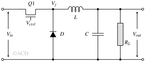
A basic buck converter comprises essential components like a switch (MOSFET or BJT), an inductor, a diode (or a second MOSFET), and a capacitor, as depicted in Fig 2. The control circuit (typically an integrated circuit) monitors the output voltage, compares it with a reference value, and autonomously adjusts the duty cycle to achieve the desired output voltage.
The fundamental configuration of a buck converter comprises the following elements:
- Inductor (L): The inductor plays a key role in storing and releasing energy during switching cycles. Its main function is to accumulate energy in its magnetic field and supply current to the load when the switch is on. When the switch is off, the inductor continues to provide energy to the load while gradually releasing the stored energy.
- Switch (Q1): The switch (typically a transistor) alternates between two states - ON and OFF. When the switch is in the ON state, it allows current to flow from the input source to the inductor. When the switch is OFF, the energy stored in the inductor is released to the output load through a diode (D) or another switch.
- Diode (D): It functions as an automatic switch. It remains off when the main switch is closed due to being reverse-biased. When the main switch turns off, it automatically turns on, allowing the inductor to release its stored energy.
- Output capacitor (C): The output capacitor is used to smooth out the ripple at the load.
- Controller IC: An integrated circuit responsible for controlling the switches ensures the desired output voltage is achieved at different load currents. It also has a lot of safety and reliability features.
Operating principle of Buck converter
In this section, a Non-synchronous buck converter is discussed. It is the foundation of the buck converter topologies. The operation can be understood by analyzing the condition of the switch when it is ON or OFF separately. The input voltage is always higher than the output voltage.
Switch in ON

In a buck converter, when the switch (typically a MOSFET) is turned on, current flows from the input source to the output load through the inductor. Diode D1 is reverse-biased because the cathode voltage is higher than the anode voltage.
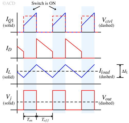
During this phase, current builds up in the inductor (as shown in Fig. 4). The inductor stores energy in a magnetic field and resists sudden changes in current. Energy from the input source is transferred to the inductor during this ON period. The voltage across the inductor is the difference between the input and output voltage, as shown in Fig. 3, assuming that the voltage drop across the switch Q1 is negligible.
$$\Delta{}I_{L}=\cfrac{V_{in}-V_{out}}{L}T_{on}$$
The capacitor (C) is used to smooth out the output waveform and reduce the ripple caused by the triangular nature of the inductor current.
The power dissipation through an ideal switch is zero (assuming zero switch resistance). Power dissipation through the diode is zero (assuming zero forward voltage drop). So, the converter has no power dissipation during the switch ON phase.
Switch is OFF
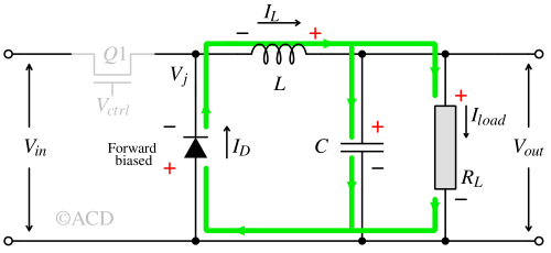
When the switch in a buck converter turns off, the inductor will still flow in the same direction. To do that, it induces a negative voltage at the cathode of the diode (Vj), turning the diode ON and forcing it to conduct.
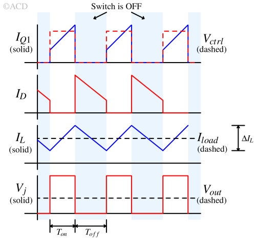
Vj is set to 0V due to the diode turning on. The inductor is bleeding energy in the form of current. The voltage across the inductor is constant, so the rate of drop in current is also constant, having a negative slope of Vout/L.
$$\Delta{}I_L=-\cfrac{V_{out}}{L}t_{off}$$
The capacitor also provides the energy to load and simultaneously get charged by the inductor's current. If the inductor's current drops to zero, it becomes discontinuous conduction mode; otherwise, it remains in continuous conduction mode.
Another way to look at buck converter operation: If the waveform of Vj is observed, it shows that it is a square wave with varying pulse width (PWM). If this waveform is passed through the LC filter (which is already there), it will produce an average voltage equal to DVin.
Buck converter equation and duty cycle
The output voltage is fixed using an IC controller. If the load is fixed, the current is also fixed. To maintain the same average current to a fixed load, the change in current through the inductor during the turn-on period has to be the same as the change in the turn-off period. It means ΔIL(on)=ΔIL(off):
$$\Delta{}I_L(on)=\Delta{}I_L(off)|$$
$$\because{} V_{out} < V_{in}$$
$$\cfrac{V_{in}-V_{out}}{L}T_{on}=-\left(\cfrac{-V_{out}}{L}T_{off}\right)$$
$$\cfrac{V_{out}}{V_{in}}=\cfrac{T_{on}}{T_{on}+T_{off}}$$
Let duty cycle is D, which is :
$$D=\cfrac{T_{on}}{T_{on}+T_{off}}$$
Therefore, the buck equation in terms of duty cycle:
$$\cfrac{V_{out}}{V_{in}}=D$$
Buck regulator integrated circuits
Some popular buck regulators in the market are :
- LM2596 (A popular legacy buck regulator)
- LMR51430 (a more efficient buck converter than LM2596)
- MP1584
- MP2338
- MC34063
Types of Buck converter
Buck converters can be classified into two categories based on how the switching is implemented :
Non-synchronous buck converter

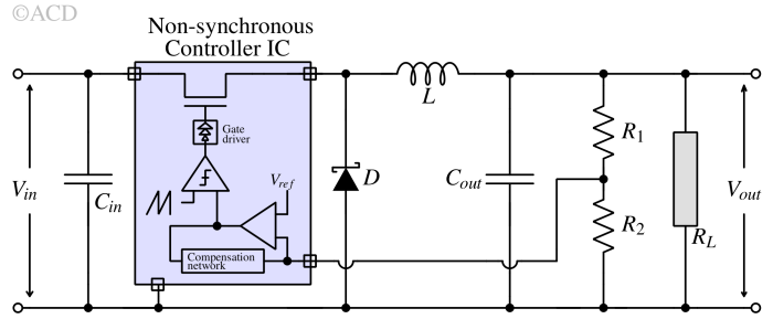
A non-synchronous buck converter has only one switch (Q1) for energizing the inductor. It depends on a diode (labeled as D in Fig. 7) to automatically turn on and de-energize the inductor when the switch (Q1) is turned off. It is simple in construction, but the efficiency is lower than the synchronous buck converter due to the higher forward voltage drop of the diode. Fig 7 shows a non-synchronous buck converter.
Synchronous Buck converter
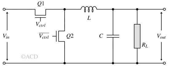
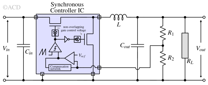
A synchronous buck converter consists of two switches (as shown in Fig 9), usually MOSFETs - a high-side (Q1) and a low-side (Q2). When Q1 is turned off, Q2 is turned on by the controller integrated circuit. Since both the switches are controlled in sync, this topology is called a synchronous buck converter.
A synchronous buck converter's main advantage is removing the diode drop when switch Q1 is off. Instead, Q2's Rds(on) carries the current with a very low voltage drop.
There is a small catch to it. The control circuit becomes complex because Q1 and Q2 should not be ON simultaneously. If not careful, a short from Vin to the ground can happen during the transition. This can cause a large current flow through Vin to ground through Q1 and Q2. This can increase dramatically increase power dissipation and reduce efficiency. This can also lead to overheating and permanent damage to Q1 and Q2. To prevent that, non-overlapping control signals are used to drive Q1 and Q2's gates. All of this is taken care of by a good controller IC.
Between the time when Q1 turns OFF and Q2 turns ON, the body diode of Q2 turns ON, allowing the current to flow. For this small moment, diode dissipation is there.
| Sr. No. | Feature | Synchronous | Non-Synchronous |
|---|---|---|---|
| 1. | Low side device | MOSFET | Diode |
| 2 | Efficiency | High | Low |
| 3 | Controller IC design complexity* | High | Low |
| 4 | Cost | High | Low |
| 5 | Power dissipation | Low (due to lower value of RDSon) | High (due to higher value of diode drop) |
* Since the controller IC takes care of the complexity internally, the buck design becomes as easy as the Non-synchronous counterpart.
Continuous and Discontinuous conduction mode
In buck converters, the current flowing through the inductor operates in two distinct modes: continuous conduction mode (CCM) and discontinuous conduction mode (DCM). Fig 4 and Fig 6 are examples of continuous conduction mode (CCM).

| Sr. No | Continuous conduction mode (CCM) | Discontinuous conduction mode (DCM) |
|---|---|---|
| 1 | The inductor current remains above zero throughout the switching cycle. The load current is higher than the average inductor current. | The inductor current drops to zero during the switching cycle when the load current is lower than the average inductor current. |
| 2 | The voltage conversion is determined solely by the input voltage and duty cycle. | The voltage conversion depends on the input voltage, duty cycle, power stage inductance, switching frequency, and output load resistance. |
| 3 | Lower EMI. | Higher EMI due to abrupt changes in current flow. |
| 4 | Lower output voltage ripple. | Higher output voltage ripple. |
| 5 | Lower stress on Switches. | Higher stress on Switches. |
Buck converters may operate in continuous conduction mode (CCM) under heavy loads and switch to discontinuous conduction mode (DCM) at light loads, known as boundary conduction mode (BCM) or critical conduction mode (CrCM). This approach combines the benefits of both modes, offering high efficiency and reduced stress, but introduces design challenges and may need more complex control schemes for stability.
Design equations and calculators
To design a buck converter, it is essential to determine the values of the capacitor, inductor, diode size, and switch size. The following parameters are required to calculate these components:
- Maximum and Minimum input voltage : (Vin,min) and (Vin,max)
- Maximum output current (Iout,max).
- Typical output voltage (Vout).
The systematic steps to find the component values are mentioned below :
- Switching frequency selection
- Inductor ripple current estimation
- Rectifier diode selection
- Controller IC selection
- Inductor selection
- Output capacitor selection
- Input capacitor selection
Switching frequency selection
The switching frequency (fs) is a critical parameter that impacts the size of the inductor and capacitors, as well as the converter's transient response, efficiency, and electromagnetic compatibility (EMC). While higher switching frequencies enable the use of smaller passive components, they can also lead to increased switching losses and reduced efficiency.
Inductor ripple current estimation
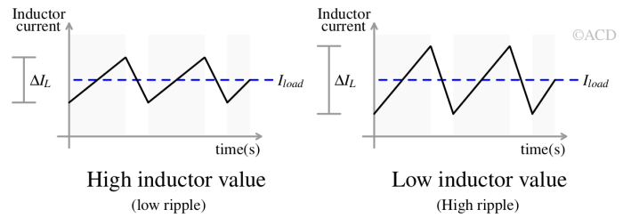
A good po\int to set the inductor ripple current (ΔIL) is 25-40% of the maximum output current (Iout). This leaves a decent margin for the inductor to stay in CCM mode and avoid going into DCM mode. In the following formula, the ripple current is fixed at 40% of the maximum load current (Iload).
$$\Delta{}I_L=0.40\times{}I_{load}$$
The ripple current gets fixed if the value of the inductor and switching frequency is already known. It can calculated using the following relation:
$$\Delta{}I_L=\cfrac{(V_{in}-V_{out})}{L\cdot{}f_s}\cfrac{V_{out}}{V_{in}}$$
Rectifier diode selection
Schottky diodes are preferred over PN junction diodes because they have a lower forward voltage drop, resulting in lower power losses.
$$I_F=I_{out,max}\times{}(1-D)$$
It is critical to select the area/size of the diode according to the forward current requirement. A smaller diode than necessary may result in a higher voltage drop and increased power dissipation.
Controller IC selection
| Sr. No | Properties | LM2596 | LMR51430 | MP2338 | MP1584 | MC34063 |
|---|---|---|---|---|---|---|
| 1 | Switching frequency | 150 kHz | 0.5/1.1MHz | 450 kHz | 1.5 MHz | 100 kHz |
| 2 | Current rating | 3 A | 3A | 3 A | 3 A | 1.5 A |
| 3 | Input voltage | 4.5V - 45V | 4.5V - 36V | 4.5V - 28V | 4.5 - 28V | 3V - 40V |
| 4 | Synchronous/Non-synchronous | Non-Synchronous | Synchronous | Synchronous | Non-Synchronous | Non-Synchronous |
| 5 | Thermal shutdown | Yes | Yes | Yes | Yes | No |
| 6 | Short circuit protection | Yes | Yes | Yes | Yes | Yes |
| 7 | In-rush current protection (soft-start) | Yes | Yes | Yes | Yes | No |
| 8 | Typical Efficiency (Vin\=12V and Iload = 500mA) | 85% | 94% | 95% | 87% | 83% |
Input capacitor and Input voltage ripple
An input capacitor is essential to counteract the effects of trace inductances in the input lines. At the switching frequency, these inductances can cause voltage ripple. Placing an input capacitor near the input pin of the buck converter helps suppress this input ripple voltage effectively.
$$V_{irpp}=\cfrac{I_{load}}{f_s\cdot{}C_{in}}\cfrac{V_{out}}{V_{in}}\left(1-\cfrac{V_{out}}{V_{in}}\right)$$
The datasheet typically specifies the minimum value for the input capacitor. For optimal performance, low-equivalent series resistance (ESR) ceramic capacitors with a dielectric material of X5R or better are recommended to prevent significant capacitance loss due to DC bias or temperature variations.
Inductor selection
The inductor value (L) should be selected to optimize the trade-offs among output voltage ripple, transient response, and physical size. It can be determined using the following formula:
$$L=\cfrac{(V_{in}-V_{out})}{\Delta{}I_L\cdot{}f_s}\cfrac{V_{out}}{V_{in}}$$
Output capacitor and Output voltage ripple
The value of the output capacitor (Cout) is determined by the maximum tolerable output voltage ripple (Vorpp).
$$V_{orpp}=\Delta{}I_L\left(R_{esr}+\cfrac{1}{8\cdot{}f_s\cdot{}C_{out}}\right)$$