D Latch and D Flip-Flop
Both the D Latch and D Flip-Flop are essential memory elements in digital electronics used to store a single bit of data (1 or 0). While they look similar in logic diagrams, the way they respond to a clock or enable signal is fundamentally different.
What is a D latch?
A D latch is a type of digital circuit that can store one bit of information with one input (D for data/delay) and enable signal (CLK or EN). The output of the latch follows the input D when CLK is high and holds its value when CLK is low. It can be thought of as a basic memory cell that can be set or reset by the data input.
D latch from an SR latch
The Delay latch (D-Latch) can be designed using a gated SR latch with an inverter (NOT gate) connected between the inputs allowing for a single input D (Data). It ensures that at the same time, both the inputs, i.e., S and R, are never equal to 1, thus avoiding the forbidden state in S R latch. The D latch is the most important and most popular latch from other clocked types. This is because it is requires least number of components and has very simple working principle.
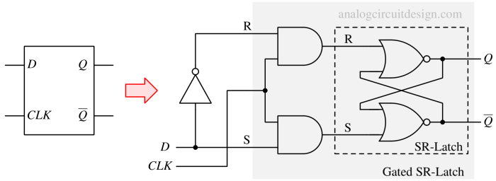
D latch can be created using an SR latch. It is done by connecting the D input to the Set (S) input, not-D to the Reset (R) input and use the clock signal to simultaneously activate both the Set and Reset inputs using AND gates. This configuration ensures that when the clock signal is active, the D input is transferred to the latch output, effectively creating a D latch. When clock input is low, the SR latch is in retain state and retains its previously loaded value.
D-latch from back-to-back inverters
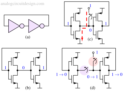
Creating D-latch from SR latch requires a greater number of components so, another way of making D-latch is widely used in electronics industry.
In Fig 2(a), back-to-back inverter is shown which can store 1 bit of data. However, without any modifications, there is no way to change the data. To understand this, let's assume that in Fig 2(b) the latch somehow has stored logic 1 at the output.
In Fig 2(c), to change the logic, a switch is introduced at the gate of second inverter. Let's call this switch, data switch. This data switch is trying to force 1 from 0 at the gate of the second inverter. However, the first inverter is trying to maintain logic 0 at the same node and the switch is forcing logic 1. So, a clear contention is present. The switch and the NMOS of first inverter are creating a very low resistance path from supply to ground which can lead to large current flow.
In Fig 2(d), to break the current flowing path, a switch is introduced between output of the first inverter and gate of the second inverter. Therefore, this switch has to be disconnected first and then the data switch has to be connected.
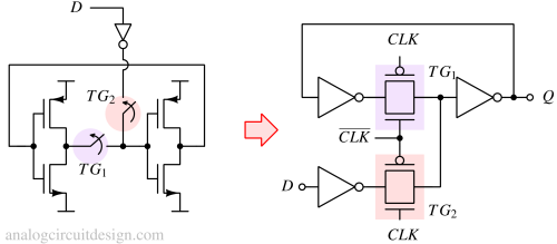
We saw in Fig 2 how a data can be loaded into back-to-back inverter-based latch. We shall add one more inverter before the data switch as shown in Fig 3. In Fig 3, the data switch is represented by TG2. TG stands for transmission gate switches. The complete circuit of the D-latch is presented in Fig 3 (\right-side).
MUX (multiplexer) based D latch
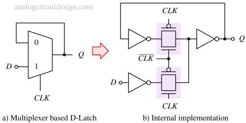
Another way to understand the origin of the D-latch is to assume it as a multiplexer. A 2 x 1 multiplexer's output can be fed back to one of its inputs (CLK=0). The other input (CLK=1) can be the D-input. The internal circuit resembles the back-to-back inverter based latch.
Truth table of D latch
| Trigger | Input | Output | |
|---|---|---|---|
| D | Q | Qn+1 | |
| 0 | X | Retain | Retain |
| 1 | 0 | 0 | 0 |
| 1 | 0 | 1 | 0 |
| 1 | 1 | 0 | 1 |
| 1 | 1 | 1 | 1 |
Excitation table of a D latch is mentioned above. D is the input, and Q is current state, Qn + 1 is the next state outputs. Qn+1 will always be 0 when D is 0 and Qn+1 will always be 1 when D is 1, irrespective of current state of flip flop. X means don't care.
The D latch is also known as a transparent latch, because when CLK is high, the output Q is transparent to the input D. This means that any changes in D will be reflected in Q immediately. However, this also means that any glitch at the input D will appear at the output during the high period of CLK, which can cause glitches or errors.
What is a D Flip-Flop?
To avoid the problem of glitches in level-triggered D-latches, a D flip-flop can be used instead. A D flip-flop is a circuit that only updates its output on the edge (rising or falling) of the clock signal, rather than on the level (high or low) of the clock signal. This ensures that the output Q only changes at discrete and predictable times. All the signal changes happen during the steady state of the clock signal where glitches may come. So, edge of the clock is the best time to capture and lock the final input.
The D (or Delay) Flip Flop serves as an electronic memory element since its output is retained unless intentionally modified by a rising edge clock signal. This flip flop is also employed to delay the change of its output signal (Q) until the subsequent rising edge of a clock timing input signal takes place.
Construction of a D Flip-flop (Master-slave)

A D flip-flop can be made by connecting two D latches in series, with inverted clock signals (as shown in Fig 5). The first latch is called the master, and the second latch is called the slave. The master latch captures the input D when CLK is high and transfers it to the slave latch CLK goes low. Now any glitch at the input won't affect the slave's output because master is disabled. This is perceived as the latch is updating its output Q on the falling edge of the clock and holds it until the next falling edge of the clock.

A positive edge-triggered D flip-flop can be made by connecting another inverter after the CLK or by rearranging the already existing inverter (shown in Fig. 6)
D Flip-Flop using S R Flip-Flop or latches

D flip-flop can be made using SR Flip-Flop by connecting a NOT gate from SET pin to RESET pin as shown in the above figure. This avoids the forbidden state in SR flip-flop and make sure that the S and R input are always opposite. Though this is one way to create a D Flip-Flop from SR Flip-Flop, the number of gates it takes is larger than the MUX based master-slave topology.
Transistor level D flip-flop
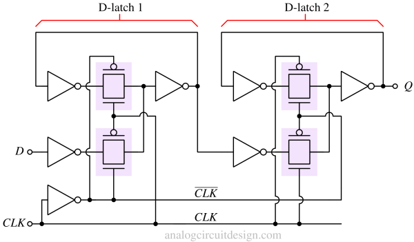
A transistor level schematic of positive edge triggered D Flip-Flop is shown in Fig 7. The transmission gate based latches (Fig 4) are used to create a D flip-flop (Fig 7). It is one of the most popular versions of D flip-flop made commercially. Additional inputs like PRESET (PRE) and CLEAR (CLR) can be added for additional functionality.
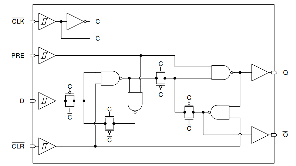
Transistor level schematic of a commercially available integrated circuit 74HC74 from Texas Instruments is shown in Figure 8. It is similar to the schematic shown in Figure 7 with additional inputs like PRE and CLR. PRE input is active low here. Meaning when PRE = 1, the data stored in the latch is 1, resulting in output Q = 1. This is used to set an initial condition to the flip-flop. For PRE to affect the internal state, it does not need to wait for clock edge. CLR clears the internal state and set the output to 0. This also does not depend on clock edge.
Applications of D Flip-Flop
- The D flip-flop is versatile in digital systems, serving roles in memory circuits, register creation, counters, and the development of synchronous systems. It is utilized for data storage, enabling flexible register sizing, counting events, and contributing to synchronous system design.
- The D Flip Flop serves as a foundational component for constructing shift registers. When eight D Flip Flops are linked sequentially, for instance, a byte (8-bits) of data can be retained following 8 clock cycles.
- Creating a basic divide-by-two circuit involves linking back the not-Q output of the D Flip Flop to its D input. This configuration results in the D output changing state at half the frequency of the clock signal. Through the successive connection of D flip flops and the careful design of external combinational logic gates, it is possible to construct a countdown timer.