Flash ADC
One of the fastest ways to convert an analog signal to a digital one is to use a Flash ADC. This type of ADC can convert very high frequencies of input signals, such as those found in oscilloscopes that operate in the GHz range. However, flash ADCs are not perfect: they consume more power than other ADCs and they are limited to low resolutions, typically up to 8 bits. This is because the number of comparators required for a flash ADC increases exponentially with the number of bits.
Architecture and Components of flash ADC
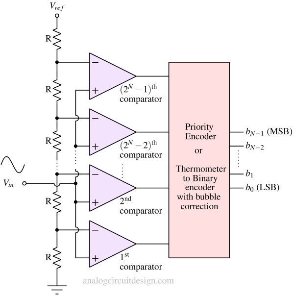
The architecture of a N-bit flash ADC is based on a set of 2N-1 comparators that measure an analog signal and convert it to a digital output. Each comparator has a unique reference voltage. The reference voltages increase linearly for each comparator. The reference voltages are generated by a resistive divider network that divides the reference voltage into 2N equal steps.
The comparators are usually arranged as a series of wideband low-gain stages. These comparators are designed to minimize voltage offset, ensuring that the input offset for each comparator is smaller than the desired LSB of the ADC. This prevents the comparator's offset falsely triggering the comparator to logic high. Each comparator's output is retained by a regenerative latch, featuring positive feedback that compels the end state to settle as either a 1 or a 0. The regenerative latch, due to positive feedback is faster than open loop architectures.

Working of a Flash-ADC
The output of each comparator is a 1 or a 0, depending on whether the analog input is higher or lower than the reference voltage. If a comparator voltage is 1, all the lower comparators' voltages are also 1 because the analog input is higher than the reference of those comparators as well. That is why the outputs of all the comparators form a thermometer code, which is then decoded to a binary code by a priority encoder.
It can be seen that the conversion (sample and quantisation) happens at the first stage only. The priority encoder is a combinational logic which introduces only propagation delay. That is why it converts the signal to digital within a single clock cycle. Nonetheless, this speed comes with a trade-off. In comparison to alternative ADC types like the successive approximation ADC or the delta-sigma ADC, the flash ADC is less precise. This discrepancy arises from the need for numerous comparators and resistors in the flash ADC, which can lead to inaccuracies from component mismatches or noise.
Sparkle codes
Typically, the outputs of the comparators form a thermometer code, for example, 00111111. However, errors may lead to patterns such as 00110111, where a stray zero appears out of sequence. This misplaced bit is referred to as a sparkle code, arising from issues like incomplete input settling or mismatched comparator timing. Such errors can result in significant deviations.
Metastability
Metastability occurs when a comparator output is indeterminate. It can be minimized by allowing more regeneration time. To handle this, outputs are often first encoded in Gray code and then optionally converted to binary.
Clock Jitter
SNR decreases with sampling clock jitter, especially at high input frequencies, so a low-jitter clock is essential for accurate ADC performance.
Applications of a Flash ADC
- Flash ADCs are a type of analog-to-digital converters that can process high-frequency signals, such as those used in radar, radio, testing, and optical systems.
- They are also used in delta-sigma modulation loops.
- Flash ADCs can store multiple bits per cell in NAND flash memory by using different voltage levels.
Drawbacks of flash ADCs
- Power Consumption: Flash ADCs consume a significant amount of power, making them unsuitable for battery-powered or low-power systems. Reducing power consumption by using lower supply voltages can compromise the dynamic range, and sub-ranging architectures can help mitigate this issue.
- On-chip/PCB area and Component Requirements: Flash ADCs require more components compared to other ADC types, resulting in larger and more complex designs. The number of comparators grows exponentially with the ADC's resolution, making it challenging to implement high-resolution flash ADCs in limited space. The use of folding architectures can help reduce size.
- Limited Resolution (DNL and INL errors): Flash ADCs have limited resolution due to the increasing number of comparators required as the resolution rises. This complexity restricts their use in applications demanding high resolution, like audio or video.