IC 741 Op Amp
The IC 741 opamp is the most popular general-purpose operational amplifier in history. Due to its legacy and availability, it is probably the best-known opamp IC. Dave Fullagar from Fairchild Semiconductor introduced this opamp IC in 1968.
The original IC 741 was named μA741 by Fairchild Semiconductor. Presently, it can be found in LM741 from Texas Instruments and STMicroelectronics. For new product developments, IC 741 can be considered obsolete because for same price and pin configuration, manufacturers are providing far better amplifiers.
IC 741 op amp pinout
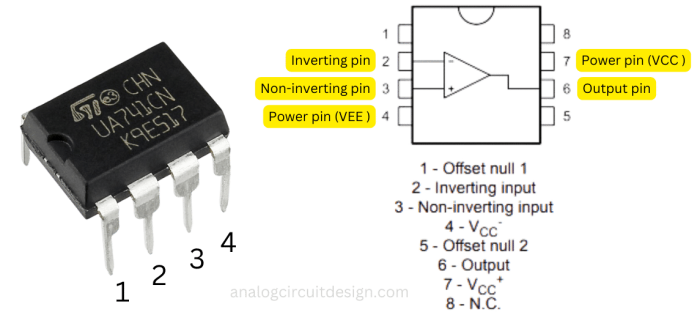
As shown in below figure, IC 741 opamp has 8 pins. Two are input pins, one is output pin, two are supply pins and two are offset null pins.

All the pins of IC 741 opamp and their functionalities are mentioned below :
- Pin 1 and Pin 5 (Offset Null): These pins are used to connect external resistors (or potentiometers) so that a small current can be injected to make the offset zero. This offset voltage is typically caused by random mismatches in the manufacturing process of the op-amp or by external factors such as temperature variations.
- Pin 2 and Pin 3 (Input): These pins are for input signals. Pin 2 is the inverting input, and Pin 3 is the non-inverting input. The output signal depends on the voltage difference between these inputs.
- Pin 4 and Pin 7 (Power Supply): These pins provide power to the IC, with Pin 7 being the positive voltage supply terminal and Pin 4 being the negative voltage supply terminal. The voltage between these two pins typically ranges from 5V to 18V.
- Pin 6 (Output): This pin outputs the amplified signal. The voltage at this pin depends on the input signals and the feedback mechanism. A high output voltage means it's close to the positive supply voltage, while a low output voltage means it's close to the negative supply voltage.
- Pin 8 (N/C): This pin is not connected (N/C) to any internal circuitry.
Key specifications of IC 741 opamp
Here are some key specifications of the 741 op-amp:
- Input Offset Voltage: The 741 op-amp has a typical input offset voltage ranging from a few millivolts to a few millivolts.
- Input Bias Current: The input bias current is typically around 80nA.
- Open Loop Gain: The open-loop gain of the 741 op-amp is typically around 100,000.
- Bandwidth: The bandwidth of the 741 op-amp is typically around 1 MHz. This 1 MHz number represents gain-bandwidth product of the opamp.
- Slew Rate: The slew rate is typically around 0.5 V/µs.
- Supply Voltage: The 741 op-amp typically operates with a dual power supply voltage range of ±5V to ±18V, though it can sometimes work with a single supply voltage if biased appropriately.
- Temperature Range: The 741 op-amp typically operates within a temperature range of 0°C to 70°C.
- Maximum output current: 20mA
If you want to learn more about the non-ideal properties of operational amplifiers, visit this page: Operational amplifier properties
IC 741 opamp internal circuit diagram
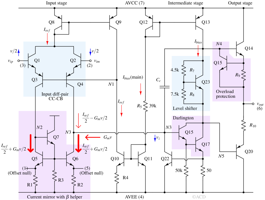
IC 741 opamp is a three-stage opamp. The first stage is the transconductance stage. It converts the input (vip - vim) into a current. The first stage comprises transistors Q1 to Q7. The second stage is a common emitter stage or a high-gain Darlington stage. The transistors Q15 and Q17 form the second stage (Darlington stage). The third stage is the buffer stage which is meant to provide current to the load and has unity gain. Transistors Q14 and Q20 form the buffer stage.

Input stage
Transistors Q1 to Q7 form the input stage. Q1 and Q3 form a compound transistor stage called CC-CB. CC means common collector, and CB means common base. Q1 and Q2 are configured in common collector mode. Q3 and Q4 are configured in common base mode.
Transistors Q8 and Q9 form a current mirror. Q8 carries the sum of currents of Q1 and Q2. Also, assuming very little current can enter the base of Q3 and Q4, the entire current Iref is flowing through Q9. Q8 is also carrying Iref current. Therefore, the sum of currents of Q1 and Q2 is Iref.
To understand the operation of the input stage, let's apply a differential voltage at the input. When vip goes up and vim goes down by magnitude v/2, there is a rise in current through Q1 and a fall in the current of Q2. However, the sum of the currents is still equal to Iref. Currents of Q5 and Q6 are the same because they form a current mirror. So, the difference between the current of Q4 and Q6 flows out of the input stage through node N3.
Benefits of using CC-CB stage
The primary benefit of employing a CC-CB (Common Collector-Common Base) based input stage lies in its immunity to phase reversal issues. Phase reversal typically arises in input stages utilizing a common-emitter configuration. Ordinarily, the collector moves in the opposite direction to the base movement. This occurs when the collector-base junction is reverse-biased. However, when the collector-base junction is forward-biased, the collector begins to follow the base, contrary to the intended behavior. By permanently tying the collector to near supply voltage, this configuration effectively resolves the phase reversal problem.
Second stage (intermediate stage)
Q15 and Q17 form the Darlington stage. Q15 provides the base current of Q17. The Darlington stage helps achieve high input impedance, increasing the amplifier's DC gain. To understand this, suppose the intermediate stage uses only Q17; the input impedance (R1) would be β(1/gm+R50). This would limit the gain (G) from the first stage to gmβ(1/gm+R50).
For example, if we take gm=1mA/V, β=100, and R50=50Ω, the value of G equals 100, around 40dB of gain. With the addition of Q15 before Q17, the input impedance becomes β2(1/gm+R50), which is β times more. So, the gain is now 80dB, which is a 40dB increase from without the Darlington pair.
The function of Q22 is to divert the current of the first stage to itself, killing gain when a large current flows through the 50-ohms resistor. This happens during short circuit or overload conditions.
Output stage (third and final stage)
The third stage is a class AB output stage. It is formed using Q14 (NPN) and Q20 (PNP) in a common collector configuration. This stage also has an overload protection circuit, which limits the output current when the output is shorted to a fixed voltage. Connecting to a fixed voltage can force the amplifier to give a large current, permanently damaging the IC. The overload protection circuit uses Q15 and R9 (25 Ω). Whenever the current through R9 is 0.7V/25Ω, it turns on Q15. Turning on Q15 removes the current from the base of Q14, limiting the current.
Applications of IC 741
Applications of IC 741 opamp :
- DC amplifiers
- Summing amplifiers
- Integrators and differentiators
- Active filters