Inverting Op-Amp
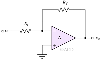
The inverting operational amplifier is a fixed-gain amplifier producing an opposite output polarity voltage for a given input voltage, as its gain is always negative.

For example, if Rf = 1000 Ω, Ri = 1000 Ω, and the input voltage is +1V, the output voltage will be -1V. The output voltage has opposite polarity and the magnitude depends on the gain. In this case, the gain magnitude is Rf/Ri = 1.
Operating principle and Inverting op amp formula
An inverting opamp works on the principle of negative feedback in the presence of a large gain of the opamp. Usually, when we refer to the gain of inverting op amp configuration (inverting amplifier), we mean closed loop gain. The open loop gain of op-amp is very high (order of 105) but varies a lot with temperature and other factors. The closed loop gain is very well controlled due to high gain of the amplifier.
We can analyse the operation of inverting op amp by considering two basic rules of ideal opamp :
- The virtual short rule: In negative feedback configuration, the inverting and non-inverting terminals have the same voltage.
- Zero input bias currents: The input terminals do not take any currents.

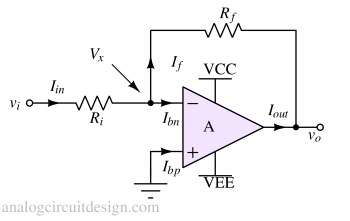
To simplify the analysis, it is fair to assume that the input bias currents Ibn and Ibp are zero (one of the above rules). Now, using KCL in node Vx,
$$\cfrac{V_x-Vi}{R_i}=\cfrac{V_o-V_x}{R_f}$$
Using the concept of virtual short in opamp, we can assume Vx = 0 (because the non-inverting terminal is connected to ground or 0),
$$V_o=-V_i\left(\cfrac{R_f}{R_i}\right)$$
Here, Ri is the resistance from the inverting pin to the ground, and Rf is the resistance from the output to the inverting pin of the amplifier.
So, the gain of an inverting amplifier can be expressed as :
$$G=\cfrac{v_o}{v_i}=-\cfrac{R_f}{R_i}$$
Note: Input bias currents, Ibn and Ibp, are usually zero for CMOS (or FET) input opamps. However, they are non-zero for BJT input opamps.
Properties of inverting opamp
- Finite input impedance (due to the presence of Ri).
- Phase inversion between input and output signal by 180°.
- The non-inverting terminal is shorted to mid-supply voltage or ground (in case of symmetric supply voltages)
Inverting op amp applications
Inverting op-amp has the following applications :
- Analog filters: It creates low-pass, high-pass, and bandpass filters using the appropriate network in place of feedback (Rf) and input (Ri) resistors.
- The voltage or current addition: Inverting op amp configuration is the building block for a summing amplifier.
- Transimpedance amplifiers: These amplifiers are used to convert the photocurrent into voltage with the help in op amp and its feedback resistor (Rf).
Stability of inverting op amp configuration
When we apply a fast voltage step at the input of the inverting amplifier, we might see ringing. This might be due to the compromised stability of the system. The stability of an inverting op-amp determines the transient response. A stable transient response means no ringing near the edges of the square wave input. A less stable system will mean ringing will be present. An unstable system would oscillate perpetually.

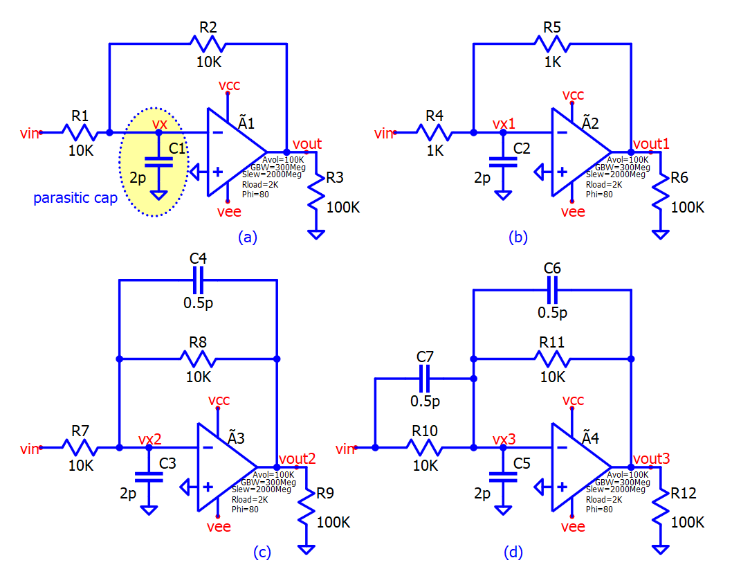
Configuration (a) in Figure 3 shows an inverting amplifier with parasitic capacitor C1. This capacitor is usually the amplifier's input impedance plus the board routing parasitic. For comparison, this parasitic capacitor is also added in other configurations. If the feedback resistor (R2) is large, it forms a pole with input capacitor (C1). Let's assume that the gain-bandwidth product of the loop gain of the amplifier is fu. So, the condition for stability is :
$$f_u\ll{}\cfrac{1}{(R_1||R_2)C_1}$$
If this condition is not met, the step response will look like the red trace (vout) shown in Fig 4. If the resistor value is decreased from 10kΩ to 1kΩ shown in circuit configuration (b) to satisfy the above stability condition. In that case, the step response will improve and look like the blue trace (vout1) in Fig 4.

Sometimes, the op-amp cannot drive low resistors present in the feedback path due to the output current specification limitations of the opamp. So, a capacitor in feedback C4 will help achieve better stability with a high resistor value, as shown in circuit configuration (c). It introduces a zero before the unity gain bandwidth of the system, which helps restore the phase margin of the system. The waveform will look like the dark-green trace (vout2) in Fig 4. It does not ring like a red trace (vout). However, the rise is slow compared to other waveforms because the configuration is similar to an active low-pass filter.
An input capacitor C7 can be placed parallel to the input resistor to improve (reduce) the rise time. The waveform is represented by light green (vout3) in Fig 4. The rise time is significantly improved compared with the dark-green trace. The waveform looks very stable in comparison with the red trace.
Additional Resources
- https://youtu.be/06xu3Mfdhfs