Level shifter circuit
In digital systems, it's common for distinct sections to function using different power supply voltages. In real circuits, problems may occur if these systems are directly connected without specialized circuits like level shifters in place.
Consider this example: When connecting an ESP8266 module, operating at 3.3V, to an Arduino UNO, a board with a 5V logic level, it becomes necessary to employ a level shifter. This level shifter facilitates the translation of signals from 5V to 3.3V and vice versa. Failing to do so risks potential damage to the ESP's silicon or incorrect readout by Arduino UNO due to incompatible voltage levels between the two devices.
Level shifter circuit diagram and design
A level shifter can be made using different techniques as mentioned in the circuit diagrams below. Each circuit topology has its own advantages and disadvantages.
Level shifter using resistor divider
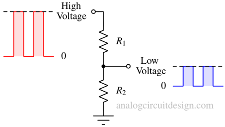
Advantages of resistor divider level shifter :
- Simple to design and easy to use
- Low cost
Disadvantages of resistor divider level shifter :
- Only capable of converting from High voltage to low voltage
- Static current dissipation versus speed tradeoff
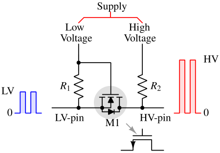
Level shifter using MOSFET (bidirectional level shifter)
Advantages :
- Simpler design than an active pull-up circuit (Fig 3).
- Low cost due to less number of components.
Disadvantages :
- Pull-up is not active. This means the rise time can be slow. However sufficient for many applications.
- Requires the driving pin to supply enough current to pull down R1 and R2 to the ground.
Level shifter cell in VLSI (active pull-up level shifter)
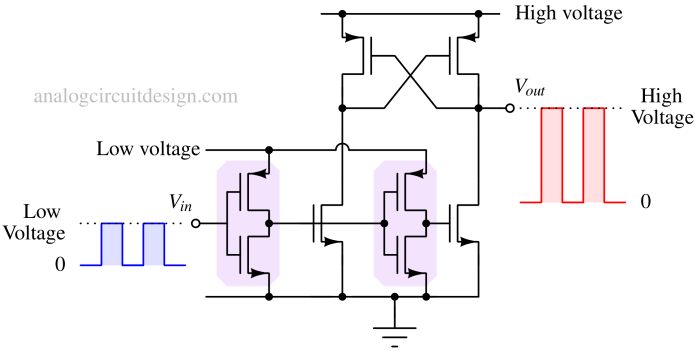
This circuit is very popular in integrated circuit design. The advantages of the circuits are :
- Zero static current (means zero static power loss).
- High speed because it has an active pull-up (using cross-coupled PMOS devices). Implementation in Fig 2 has a passive pull-up (using R2).
- Zero input current requirement. This means that the pin driving Vin node in the circuit mentioned in Fig 3 need not have high current drive capability. This is because Vin has MOSFET gates as input.
Disadvantages :
- It is unidirectional. This means the same circuit cannot level shift from high voltage to low voltage. Needs a separate circuit (but identical) with low-voltage and high-voltage sides swapped. So, not suitable for I2C buses.
- Requires more components to build.
Working principle of bidirectional level shifter
- Low voltage (3.3V) to High voltage (5V) conversion
When the LV-pin is asserted high (3.3V), the voltage difference across R1 is zero, and the VGS of the MOSFET is zero. So, no current is flowing through MOSFET. Meaning no current is flowing through resistor R2. Hence output voltage is High (5V).
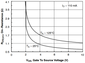
When the LV-pin is asserted low (0V), the voltage difference across R1 is 3.3V meaning VGS = 3.3V. At VGS = 3.3V, the on-drain resistance RDS(on) is ~1.5Ω (BSS138). So, the output pin forms a resistor divider and the output voltage is near 5(1.5/10000) ~ 0.75mV.
- High voltage (5V) to Low voltage (3.3V) conversion
The body terminal is internally connected to the low-voltage side so the voltage side is the source terminal of the MOSFET. Now the mechanism of turning on the MOSFET depends on the state of the body-diode and VGS. When the HV-pin is asserted low (0V), the body diode is turned on. This is because the anode is at a higher potential than the cathode. The anode terminal is also pulled down due to the HV-pin asserted low. This develops the required VGS to turn on the MOSFET. This lowers the RDS(on) (near ~ 2Ω)and the LV pin is pulled low.
When the HV-pin is asserted high, the body diode is reversed biased. Now, there is nothing to pull down LV-pin so no VGS is created and MOSFET is turned off. So, LV-pin is pulled high using 10kΩ resistor
Bidirectional level shifter working examples
Some examples of using level shifter circuits are shown below:
Level shifter 3.3V to 5.0V
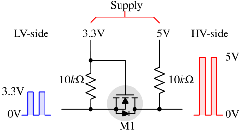
Level shifter 5.0V to 3.3V
In the above circuit, the MOSFET can be BSS138 or 2N7002/2N7000. These level shifter circuits are good for interfacing the output of Arduino UNO or any 5V output pin with 3.3V devices like Raspberry Pi, STM32, ESP8266, ESP32, Nokia 5110 LCD, etc.
Level shifter 5.0V to 12V
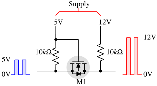
It is identical to Figure 4. The input voltage is 5V and the output voltage is 12V. The same circuit can be used to convert 12V signals to 5V signals.
Level shifter boards and integrated circuits (ICs)
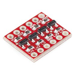
There are ready-to-use board PCBs with MOSFETs and resistor-populated which have the bidirectional level shifter implemented.
Also, there exist ICs (e.g., TXS0108E) which has similar bidirectional capabilities to the board mentioned above. However, the integrated circuit can provide more speed during pull-up as it has active pull-up capability.