Linear and Low dropout voltage regulator
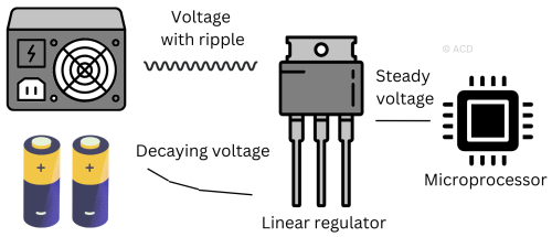
A linear voltage regulator is an integrated circuit that maintains a fixed voltage across a load independent of temperature, load current, or input voltage. It is called linear because it does not have any switching elements. For example, Lithium-polymer batteries (most commonly used in cell phones) discharge from 4.2V to 3V; however, the linear voltage regulator (low dropout voltage regulator in particular) connected to the battery’s output maintains a constant 2.5V to the microprocessor and other circuits.
Working principle of linear voltage regulator
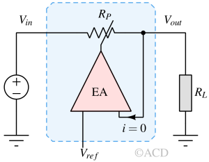
The basic principle of a linear voltage regulator is straightforward and can be understood from a resistor divider circuit, as shown in Figure 1. The resistor divider circuit is formed using RP and RL. Value of RP is controlled using an Error amplifier (EA). If RL changes, RP will also be adjusted using a feedback loop to maintain the required voltage.
$$V_{out}=\cfrac{R_L}{R_P+R_L}V_{in}$$
Linear voltage regulators features
- Only few components required for proper operation.
- No switching elements.
- LDO provides a low-noise, steady output voltage. Its ripple rejection is usually high, covering a large band (DC to a few MHz).
- Due to the significant voltage difference between input and output, the power dissipation can be high, leading to low energy efficiency.
Components of Linear voltage regulators
Main components required to make an linear voltage regulator are listed below :
Bandgap voltage reference
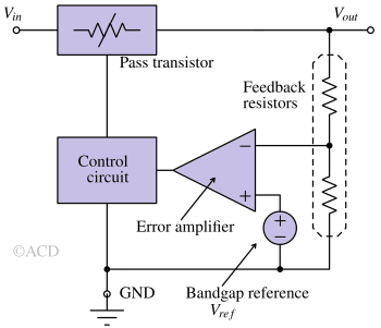
A steady reference voltage independent of temperature and supply voltage variation is generated and given as a reference to one of the error amplifier inputs. The steady-state accuracy of the LDO is very much dependent on the bandgap voltage reference. To make a bandgap reference, we add the correct proportion of PTAT (proportional to absolute temperature) and CTAT (complementary to absolute temperature) current to get a ZTAT (zero to absolute temperature).
Error amplifier
It is a high-gain DC-coupled amplifier that minimizes the error between reference and output voltage. The output of the error amplifier drives the gate/base of the pass transistor. The error amplifier's random and systematic offset determines the output voltage accuracy and drift with respect to temperature.
Pass transistor
This is the primary current-carrying device inside the regulator. It may be the NPN-Darlington pair, Sziklai pair, PMOS, or NMOS device. Bipolar devices are rugged because they lack gate oxide, unlike MOS devices.
Feedback resistor network
The internal bandgap reference generates around 1.25V. To achieve higher output voltage, we need to have feedback resistor network to amplify the output. The error amplifier is configured as non-inverting stage.
Short circuit/overload protection
This feature protects the regulator's internal devices by turning off the primary current supplying them when excessive current is sensed. Some LDOs have a thermal shutdown feature. When the temperature of the die exceeds a limit, it turns off the output device.
Difference between linear and Switching regulators
There are some basic differences between linear and switching regulators (switch mode power supplies) :
| Features | Linear regulator | Switching regulator |
|---|---|---|
| Step-down conversion | Possible | Possible |
| Step-up conversion | Not possible | Possible |
| Inverting conversion | Not possible | Possible |
| Design complexity | Simple | Complex |
| External components | Few | Many |
| Efficiency | Less | High |
| Output voltage ripple | Very small | Large |
| Heat generation | Large | Small |
Types of linear voltage regulators
- Standard dropout voltage regulators (e.g., LM317, LM7805, LM7812)
- Low dropout voltage regulators (e.g., LM1117)
Standard dropout voltage regulators
These are classic voltage regulators (standard voltage regulators) commonly using a Darlington NPN-type transistor (e.g., LM7805), a Sziklai pair (e.g., LM317), or an N-channel MOSFET as an output pass transistor.
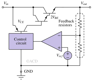
As shown in figure above, an input to output voltage difference is called a dropout voltage (VDO) which is necessary to achieve the desired output voltage and expected load and line regulation. In the case of Darlington NPN-type voltage regulators, the minimum value of VDO must satisfy :
$$V_{in}-V_{out}>2V_{BE}+V_{CE,min}$$
Low dropout voltage regulators (LDOs)
In contrast to standard regulators, LDO regulators mainly use a PNP transistor or a P-channel MOSFET as an output transistor. The minimum dropout voltage of such LDO regulators is determined by the collector-emitter voltage (VCE(sat)) or the drain-source voltage (VDS = RDS(ON) × ID). The minimum dropout voltage can be 250 mV. 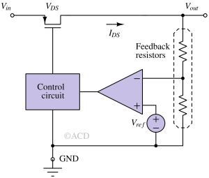
This low dropout significantly increases the power efficiency, sometimes beyond 95%. Nowadays, the most power-efficient design uses LDOs.
Efficiency of linear regulators
Efficiency of a regulator can be expressed as :
$$\eta{}=\cfrac{\text{Output power}}{\text{Input power}}=\cfrac{V_{out}*I_{load}}{V_{in}*(I_{load}+I_Q)}$$
For example, if input is 12V, output is 5V and Iload = 100mA, efficiency is :
$$\eta{}=\cfrac{5\times{}0.1}{12\times{}0.1+12\times{}0.004}\times{}100=32%$$
The efficiency is 32%, which is considered very low. For portable (battery operated) applications, anything below 90% efficiency is unacceptable.
Improving the efficiency of linear regulators by using LDOs
The efficiency is low in linear regulator if the input voltage is significantly higher than the output voltage. Switching regulators are very efficient when having large input voltage with relatively small output voltage. So, a switching buck regulator can be used to bring the input voltage down for the linear regulator. Let's consider switching regulator to be 100% efficient.

So, if the output voltage requirement is 5V, the input voltage should be 5+VDO for best efficiency. VDO is the minimum dropout voltage of the linear regulator. The output of switching regulator should be 5+VDO. The efficiency can be expressed as :
$$\eta{}=\cfrac{5*I_{load}}{(5+V_{DO})*(I_{load}+I_Q)}$$
So, from above equation, we can say that efficiency is higher when VDO (dropout voltage) is small. That is why low dropout voltage regulators (LDO) are needed. LDOs have a dropout voltage ranging from 0.25V to 1V.
Fixed and Adjustable linear voltage regulators
Voltage regulators are available in both fixed and adjustable variants.
Fixed voltage regulators
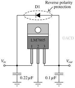
Fixed voltage regulators produces a fixed DC output voltage, which is either positive or negative. These regulators do not need extra feedback resistors at the output.
78xx voltage regulator ICs (e.g., 7805, 7812) produce positive fixed DC voltage values and 79xx voltage regulator ICs produce negative fixed DC voltage values. For 79xx voltage regulators (e.g., 7905), the input should be negative as well.
Adjustable voltage regulators
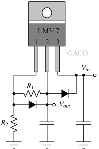 An adjustable voltage regulator produces a DC output voltage, which can be adjusted to any other value by changing the value of feedback resistors (R1 and R2). LM317, LT1086, LM1117 are some adjustable voltage regulators. These regulators are capable of generating positive voltage. LM337 is a negative voltage regulator. It needs a negative input for desired operation.
Terms related to standard and low dropout voltage regulators
Load regulation
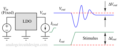
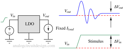
Load regulation is an amount of change of output voltage (VOUT) with respect to load current when the input voltage (VIN) is kept constant. Linear voltage regulators with a smaller load regulation value have a higher ability to maintain a regulated output voltage (VOUT) despite changes to the output current (IOUT). If the output current range is wide, it is necessary to use an linear voltage regulator with a smaller load regulation value.
$$\text{Load regulation}=\cfrac{\Delta{}V_{out}}{\Delta{}I_{out}}$$
Line regulation
Line regulation is an amount of change of VOUT with respect to VIN when the load current is kept constant. LDOs with a smaller line regulation value have a better ability to maintain a regulated output voltage (VOUT) despite changes to the input voltage (VIN). If it is known that the input voltage can vary a lot, it is necessary to use an LDO with a small line regulation value.
$$\text{Line regulation}=\cfrac{\Delta{}V_{out}}{\Delta{}V_{in}}$$
Dropout voltage (VDO)
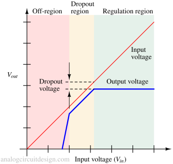
The dropout voltage is the minimum difference between input and output voltage of LDO at which it can perform to desired specifications. The major difference between a standard voltage regulator and a low dropout regulator is the pass transistor. A minimum dropout is required for the functionality of the pass transistor. The dropout voltage of an LDO with a MOS output transistor is specified under the conditions in which the MOS output transistor is operating in the pinch-off region.
| Sr. No | Linear regulator name | Dropout voltage (VDO) |
|---|---|---|
| 1 | LM7805 | 2V |
| 2 | LM317 | 3V |
| 3 | AMS1117 | 1.1V |
| 4 | TPS7A54 | 0.2V |
Quiescent current (IQ)
It is the current consumed by the LDO itself. This current is necessary for the functionality and performance of the LDO.
In some architectures (eg., BJT-based pass transistor), the quiescent current increases with load current. In MOS based pass transistor, the quiescent current remains same with load current.
Current limiting (ICL)
If the output current has become too high, it may damage the pass transistor device inside the LDO due to temperature rise. So, there is an internal circuit that senses the current and the output current is limited as soon as the current limit threshold is reached.
Undervoltage lockout (UVLO)
If the input supply voltage is lesser than some threshold voltage, the device remains in power down. This is necessary because the LDO may not regulate the output in such conditions or the load may not function well at low voltages.
This feature is especially very important in battery-operated devices because the battery voltage reduces with time and usage.
The following things can happen in case of Undervoltage :
- The bandgap voltage reference may not generate the expected voltage due to a supply crunch.
- Digital logic circuits may go into a tristate or metastable state.
- LDO may go out of regulation.
Power supply rejection ratio (PSRR)
It is the ratio of change (in form of ripple) in input voltage (power supply) to change in output voltage. Ideally, this value should be infinite because there should be no change in output if the input has any change in it. Most of the time the ratio is represented in dB.
$$\text{PSRR} = 20log{}_{10}\cfrac{\Delta{}V_{input}}{\Delta{}V_{output}}$$
The PSRR is a very critical parameter in audio and RF applications. Following are some major sources of ripple at the input of an LDO :
- 50Hz/60Hz ac noise.
- Switching converter ripple.
- Sharing of input voltage of LDO with digital heavy circuits.
Output noise voltage
Noise of LDO matters when the output of the LDO is directly connected to some sensors. Such sensors could be photodiode, LED etc. Some noise sources are :
- 1/f noise (pink noise): It is caused by defects on the semiconductor surface.
- Popcorn noise (burst noise): It is considered to be caused by lattice defects in the semiconductor. The name "popcorn" comes from the fact that it produces an acoustic noise that sounds like popping popcorn when it enters an audio speaker.
- Thermal noise (white noise): It is caused by random thermal movements of electrons.
- Shot noise: It occurs whenever carriers cross the potential barrier of a p-n junction.
These noises are important in the case of LDO powering up a low noise amplifier or precision signal chain.
Thermal shutdown temperature and hysterisis
Sometimes the temperature of an LDO rises beyond its junction temperature (maybe due to a short circuit at the output). In such a case, the active devices inside the LDO can get permanently damaged or there may be a degradation in performance. The load may also malfunction because of LDO destruction.
In such a case, if the junction temperature rises above the threshold, the LDO is turned off. Since the LDO is turned off, the temperature will fall now. To ensure that the LDO does not turn on immediately, a hysteretic comparator is used. Now when the junction temperature goes below a safe operating value, LDO should turn on again.
Inrush current suppression
Before system power-up, almost all capacitors are discharged. During power-on, if the voltage across the capacitor is built up very fast, it demands a large amount of current (called inrush current) from the supply. Due to wire resistances, the voltage in the power line may drop and cause system malfunction.
To avoid that, the voltage across a capacitor (which is connected to the output of the LDO) is slowly ramped up to the desired voltage to reduce this current.
Protection against reverse bias
In a linear voltage regulator, it is required that the input voltage is always higher than the output voltage.
Sometimes, when the load is turned off and the input to the LDO is turned off, the output capacitor is still charged to some voltage. At this point, the output voltage is higher than the input voltage which can stress the pass transistor.
This situation can stress the base-emitter voltage in the BJT-based pass transistors (e.g., NPN). The bulk diode can turn on and carry the stress current in a MOS-based pass transistor. The body diode may or may not be sufficient to hold that current and can get degraded.
So, an effective way to solve this problem is to add an external bypass diode (preferably a Schottky diode) in parallel with input-output. The bypass diode should be fast enough to turn on before the internal circuit (body diode of MOS or breakdown of NPN).