LM317 Adjustable voltage regulator
LM317 is an easy-to-use three-terminal adjustable-voltage regulator. The LM317 voltage regulator circuit requires only two external resistors to set the output voltage. If a fixed resistor is connected between the output and adjustment pin, it can also be a precision current regulator. Bob Dobkin designed it in 1976 while he worked at National Semiconductor. The main difference between LM317 and LM7805 is that the output voltage is adjustable in LM317 while not in LM7805. There exists LM337 for negative voltage regulation.
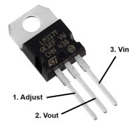
Features of LM317 voltage regulator
- It has a minimum output voltage of 1.25V. So it can be easily used for microcontrollers with 3.3V.
- The maximum output current is 1.5A.
- The minimum dropout voltage is 3V. So, it is not very efficient for low output voltages. Better alternatives could be some LDOs.
- It has more than 60dB ripple rejection for frequencies less than 10KHz. For higher frequency, it starts degrading.
- Instead of buying different fixed voltage regulators for various voltages, multiple LM317s can be purchased together. This can save cost and design effort.
Application circuit of LM317 voltage regulator
Because of the inner circuit mechanism, LM317 will try to maintain 1.25V across R1. Vout will provide the current through R1, flowing through R2 to create an additional voltage drop above 1.25V.
$$V_{out}=V_{ref}\left(1+frac{R_2}{R_1}\right)+I_{adj}R_2$$
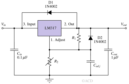
Some points to remember :
- Iadj ~ 50 μA can be negligible if current through R1 is much greater than 50 μA.
- R1 and R2 are required to set the output voltage. R2 can be a potentiometer for variable power supply applications.
- CADJ (~10uF) is added to improve ripple rejection. It prevents the ripple from amplification as the output voltage is adjusted higher. At high frequency, CADJ acts as a short to ground.
- Ci is recommended if the regulator is not near the power-supply filter capacitors. Long traces of conductors usually add parasitic inductors to the input. Ci is added to provide a high-frequency, low-impedance path to the ground, improving stability. A 0.1-μF or 1-μF capacitor gives sufficient bypassing to most applications.
- Cout improves load transient response. The internal circuit loop takes some time to respond. Meanwhile, Cout provides the necessary.
- If CADJ is used, protection diode D2 is recommended. The diode provides a low-impedance discharge path to prevent the capacitor from discharging into the regulator's output.
- Protection diode D1 is recommended if Cout is used. The diode protects internal transistors when Cout is charged and input is suddenly zero. The diode takes all the current and limits the voltage drop to 0.7-0.8V
Constant voltage with current limit
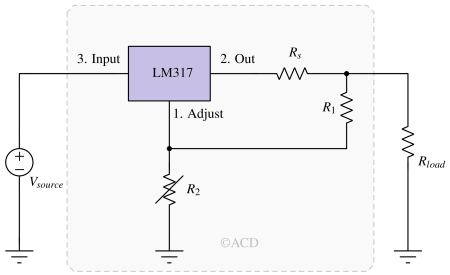
This circuit adds an Rs = 1 Ω resistor in a high-current path. The rest of the circuit is the same as the previous application circuit. When the current is low, the drop across Rs is negligible, but when the current is high, the drop across the Rs Ohm resistor becomes significant. The sum of the voltage drop across Rs and R1 is always 1.25V.
Constant current output circuit
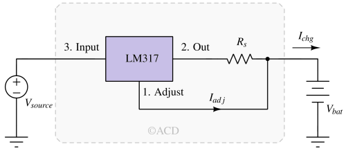
The current limit operation mode can provide a constant current at the output. The adjust pin has to directly connected to output across a resistor Rs. The LM317 will maintain 1.25V across Rs (Fig 4). To maintain this voltage, a current Ichg = 1.25/Rs has to flow. This current Ichg can be used to trickle charge a battery. Ichg = 1.25 V ÷ 100 Ω. Vsource should be greater than VBAT + 4.25 V. (1.25 V [internal reference] + 3 V [minimum dropout of LM317])
Efficiency and Heat dissipation of LM317 voltage regulator
$$\text{Efficiency}(\eta{})=\cfrac{\text{Output Power}}{\text{Input Power}}=\cfrac{V_{out}I_{load}}{V_{in}(I_{load}+I_Q)}$$
For example, if input is 12V, output is 3.3V and Iload = 50 mA, efficiency is :
$$\eta{}=\cfrac{3.3times{}0.05}{12times{}0.05}times{}100=27.5%$$
The efficiency is 27.5%, which is very low. The efficiency is low because there is a 12-3.3=8.7V voltage drop across the LM317 regulator. This voltage drop, along with the output current, consumes power, which is dissipated in the form of heat. To improve efficiency, we can use a buck-switching regulator to bring 12V to near 3.3V and then use an LDO to generate a stable 3.3V. With this methodology, the efficiency can be improved beyond 95%.
The internal circuit of the LM317 adjustable voltage regulator
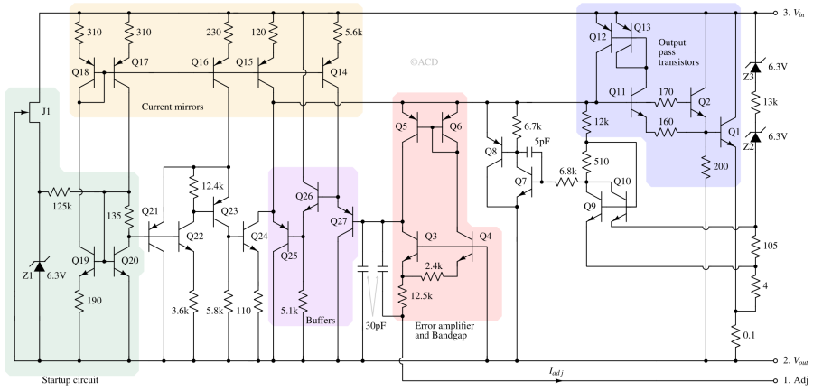
Startup circuit
As shown in Figure 5, JFET J1 with 125 kΩ resistor and Q20 transistor forms a supply-independent current source that always turns on when Vin-Vout is more than 2V. This current is mirrored and replicated in proportions across the current mirrors to supply necessary currents in the rest of the circuit.
Output pass transistors
Transistors Q1 and Q2 form the output pass transistor. These are configured as a Darlington pair. These are largest transistors inside the chip so that heat dissipation is efficient.
Dropout voltage of LM317
For the desired performance, a minimum of 3V headroom is needed across temperature and high load current. Transistor Q1 and Q2’s VBE will reach 1.1V each at cold and high currents. We need some VCE margin for Q15 and Rdegen across 120 Ohms resistors.
Error amplifier and bandgap
Transistors Q3, Q4, Q5, and Q6 form the error amplifier, and a 1.25V temperature-independent reference is maintained across pins Vout and Adj. The error amplifier detects any change at the output voltage and influences node n1 to adjust Vout to maintain Vout - Vadj = 1.25V.
Buffers and level shifters
Transistors Q25, Q26, and Q27 form buffers and level shifters. Buffer Q27 helps provide high impedance at node n2, while transistor Q25 drives the base current of Q2 and Q11. Transistors Q11, along with Q12 and Q13 try to compensate for the excessive base current requirements at high load conditions.
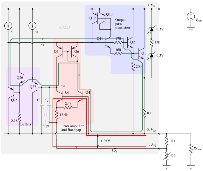
The above figure (Fig 6) simplifies LM317’s internal circuit for understanding. Transistors Q5 and Q6 carry the same current, which means that Q3 and Q4 carry the same current. Q4 is N times larger than Q3. The voltage difference across 2.4k resistor is :
$$V_{2.4k}=V_{BE,Q3}-V_{BE,Q4}$$
$$V_{2.4k}=V_t.ln{\left(\cfrac{I}{I_s}\right)}-V_t.ln{\left(\cfrac{I}{NI_s}\right)}=V_t.ln{N}=\cfrac{kT}{q}ln{N}$$
So, the voltage and current for a 2.4k resistor are PTAT (proportional to absolute temperature). We just established that the current through Q3 and Q4 are the same. So, the current through the 12.5k resistor is the sum of Q3 and Q4’s current. So, the voltage from the Adj pin to the Vout pin can be written as :
$$V_{adj}+\cfrac{12.5\text{k}\Omega{}times{}2times{}(kT/q)ln{N}}{2.4\text{k}\Omega{}}+V_{BE,Q3}=V_{out}$$
$$V_{out}-V_{adj}=\underbrace{V_{BE,Q3}}_{CTAT}+\underbrace{\cfrac{12.5\text{k}\Omega{}times{}2times{}(kT/q)ln{N}}{2.4\text{k}\Omega{}}}_{PTAT}$$
VBE,Q3 is a CTAT (complementary to absolute temperature) voltage. The other term is a PTAT voltage. The summation voltage (~1.25V) remains constant throughout the temperature range. This voltage equals 1.25V at 0K, where the PTAT term becomes zero, and the CTAT term becomes 1.25V.
Applications of LM317 adjustable voltage regulator
- HVAC: heating, ventilating, and air conditioning.
- High-speed data acquisition and generation.
- ECG electrocardiograms.
- Motor control.
- Microcontroller local supply voltage.
- Signal and waveform generation.
- Refrigeration.
- Software-defined radios.