7805 voltage regulator
7805 voltage is a commonly used linear voltage regulator regulating the output voltage to a fixed 5V. Though it is not the most efficient voltage regulator, it is a readily available IC. Suppose we have a 12V supply and require a microcontroller to be powered at 5V. Then, LM7805 is a speedy and low-cost solution. It is called linear because it does not use on-off switching to control the output voltage. There are other similar ICs, like 7809 (9V), 7812 (12V), and 7815 (15V), which have similar functionality.
Key takeaways
- LM7805 Overview: A linear voltage regulator providing a stable 5V output, commonly used for DC power supplies.
- Pin Configuration: Three pins—Input, Ground, and Output.
- Efficiency Limitations: Only ~33% efficiency in some setups due to heat dissipation.
- Improvements: Using with buck converters or switching to low-dropout regulators (LDOs) can enhance efficiency.
- Thermal Management: Importance of heat sinks for high-power scenarios.
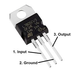
7805 pin configuration
LM7805 has a three-pins:
- Pin – 1: Input pin to connect to supply. (> 7V)
- Pin – 2: Ground pin.
- Pin – 3: Output pin which has regulated 5V output.
7805 voltage regulator application circuit
The connections are simple in the case of fixed output LM7805, as shown in the following figure. Capacitors are added to improve ripple rejection and stability (transient response). A diode is added from input to output to protect against reverse polarity.
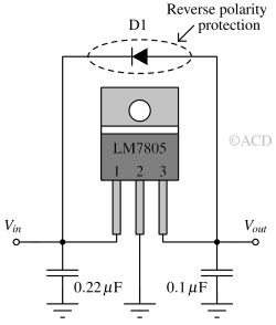
Reverse polarity protection
Diode D1 is connected to the output to protect the IC when the input is very low compared to the output. This situation is prevalent when the input is turned off (made zero), and the output capacitors are still charged to 5V. This stresses the internal pass-transistor (Q1 in the figure), causing a reverse base-emitter voltage breakdown. During regular operation (the input is higher than the output), the diode is reversed bias (turned off). During reverse polarity, it will clamp the input to the output voltage to -0.7V, protecting the internal transistors. All the output capacitor current will flow through the protection diode.
Input and output capacitors for the 7805 circuit
Input capacitor: The primary purpose of an input capacitor is to supply high-frequency current that the LDO cannot draw directly from the power source because of the inductance in the power supply line. It helps stabilize the LDO by providing an AC short to ground from the LDO’s power supply. If the capacitor is not added, the high-frequency input ripple will increase and compromise the stability of the LDO. For a 7805 regulator, a 0.22uF capacitor is typically suitable.
Output capacitor: The output capacitor plays a vital role in ensuring the stability of the LDO. It stores charge to manage sudden load current fluctuations, helping minimize output voltage ripple and noise. Additionally, it creates a pole with the LDO's output impedance, which can influence the regulator's phase margin and overall stability. The output capacitor's value and type significantly affect the LDO's transient response and stability. For a 7805 regulator, at least 0.1uF is needed.
7805 IC general features
- Output Current up to 1.5A.
- Quiescent current: 4.2mA
- Thermal-Overload Protection
- Short-Circuit Current Limiting at 750mA
- A thermal dissipative pad
- Output voltage range: 4.75V to 5.25V
- Ripple rejection (from input to output): 78dB at 120Hz
- Output noise: 40uV (integrated noise from 10Hz to 100kHz)
Efficiency of 7805 regulator and improvements
Efficiency of a voltage regulator can be expressed as :
$$\eta{}=\cfrac{\text{Output power}}{\text{Input power}}=\cfrac{V_{out}*I_{load}}{V_{in}*(I_{load}+I_Q)}$$
For example, if input is 15V, output is 5V and Iload = 500mA, efficiency is :
$$\eta{}=\cfrac{5\times{}0.5}{15\times{}0.5+15\times{}0.004}\times{}100=33%$$
The efficiency is 33%, which is considered very low. For battery-operated applications, anything below 90% efficiency is unacceptable.
Improving efficiency
A buck-switching regulator is recommended to improve efficiency. Modern switching regulators are 90-98% efficient. However, any kind of switching regulator has ripples at the output. A 7805 linear regulator can suppress the ripples because it has a high PSRR ranging from DC to switching frequency and some of its harmonics.
 For example, to get 5V from 15V, a buck converter can be used to convert 15V to 7V. Then, a 7805 regulator IC can be used to get 5V from 7V. Let’s calculate the new efficiency (assuming the buck converter is 100% efficient):
$$\eta{}=\cfrac{5\times{}0.5}{7\times{}0.5+7\times{}0.004}\times{}100=71%$$
With this topology, the efficiency improved from 33% to 71%. However, it is still not acceptable for battery-operated applications. What is limiting is the large 2V dropout voltage of 7805 IC. The efficiency can be increased to above 90% by replacing 7805 with a Low dropout regulator (LDO) like TPS7A54. This LDO can operate at a dropout voltage of only 0.2V, which is considered very good. This means that to provide an output of 5V, the input voltage needs to be only 5.2V. So, the new efficiency would be (IQ of TPS7A54 is ~3mA) :
$$\eta{}=\cfrac{5\times{}0.5}{5.2\times{}0.5+5.2\times{}0.003}\times{}100=96%$$
By replacing 7805 with an LDO, we have improved efficiency from 71% to 96%. This will increase the battery standby time and lifetime.
Heat dissipation of 7805 voltage regulator
Power dissipation inside the IC can be calculated using the following formula :
$$P_{heat}=(V_{in}-V_{out})I_{load}$$
Linear regulators like the 7805 voltage regulator dissipate heat depending on the input and output voltage difference. For example, if the input voltage is 15V, the output voltage is 5V, and the current drawn is 500mA, then the power dissipation would be:
$$P_{heat}=(15-5)\text{V}\times{}0.5\text{A}=5\text{W}$$
The LM7805 datasheet mentions thermal resistance to ambient, θja ~ 20°C/W. So, the estimated rise in the semiconductor’s junction temperature is 5W*20°C/W=100°C. If the operating temperature is 25°C, the junction temperature will be 25°C+100°C=125°C. The junction temperature range mentioned in the datasheet is 0°C-125°C. So, we are just at the edge of maximum junction temperature. With high junction temperature, the properties of the semiconductor degrade (e.g., regulation, accuracy, etc.). Also, it accelerates device aging, which can lead to failure soon.
A heat sink can be added to the semiconductor die to limit the rise in junction temperature, dropping the thermal resistance to 3°C/W. With this technique, the regulator can be expected to perform well. However, its power efficiency remains unchanged. A buck converter can be used to improve power efficiency.
7805 voltage regulator internal circuit diagram
The official circuit diagram is mentioned below :
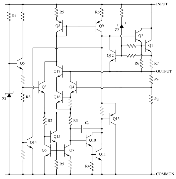
Q1 is the main transistor providing current to the output. Transistor Q2 supplies Q1's base current. Q1 and Q2 together form a Darlington pair. Diode Z2 protects transistor Q1 from reverse polarity. Transistor Q12 limits current to 750mA during short circuit conditions. Transistors Q8 and Q9 form a current mirror.
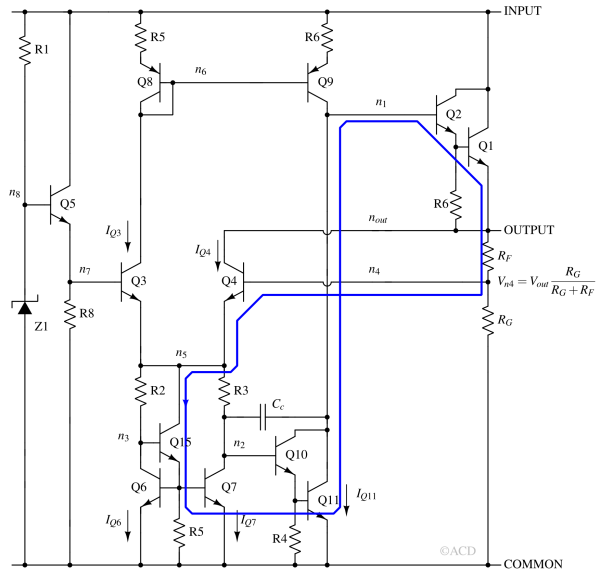
We can assume the greyed resistors are shorted to understand the operation. Q3 and Q4 form a differential pair and are identical in size. Diode Z1 and transistor Q5 form a reference, which goes as an input to Q3. The base of Q2 is called a high-Z node. This is because the input impedance of this node is very high, giving us the desired closed-loop gain. Q14 is added to protect the output from any surge voltage. The transistor pairs (Q15, Q6) and (Q10, Q11) form the Darlington pair. Q6 and Q7 form a current mirror. This means that the current through Q6 and Q7 are the same. Q8 and Q9 form a current mirror with R5 and R6 as degen resistors. The sizes Q11, Q6, and Q7 are kept identical. Similarly, the sizes of Q15 and Q10 are kept the same.
Why is the dropout voltage in the 7805 regulator high?
The dropout voltage in 7805 is high because of the usage of the Darlington pair (formed by Q2 and Q1) at the output. The Darlington pair will take up 0.8V+0.8V=1.6V of headroom. We need some VCE(sat) ~ 0.2V and Vdegen=0.2V (across R6). So, 2V of the drop is needed for proper operation. Otherwise, Q9 will saturate, leading to inaccurate output.
The internal operation of the 7805 voltage regulator
Let’s try to understand this using a simplified version of 7805 IC’s internal schematic, which is mentioned below. We have removed all the protection circuits for brevity.
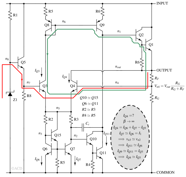
The path mentioned in red sets the voltage at the output. We can write a KVL equation to arrive at the output voltage :
$$V_{out}\cfrac{R_G}{R_G+R_F}=V_{z1}-V_{BE,Q5}-V_{BE,Q3}+V_{BE,Q4}$$
The path mentioned in green is the inner loop, which ensures that IQ4\=IQ3. That means VBE,Q3 = VBE,Q4. Therefore Vout,
$$V_{out}=\left(1+\cfrac{R_F}{R_G}\right)\left(V_{z1}-V_{BE,Q5}\right)\simeq{}5\text{V}$$
We have assumed that gm,Q3 >> 1/R2. Otherwise, another loop would be active. The other loop is mentioned in the following figure.
Advantages and Disadvantages of 7805 voltage regulator
Advantages :
- Easy to use
- Very afforable
- Package comes with heat sink
Disadvantges :
- Poor efficiency
- High dropout voltage
- Large size