Multiplexers (MUX)
A Multiplexer (or MUX), sometimes referred to as a data selector, operates by choosing among multiple analog or digital input signals and directing the chosen input to a single output line. This selection process is governed by a separate collection of digital inputs termed select lines. Specifically, a multiplexer comprising 2N inputs necessitates N select lines. A multiplexer possesses the capability to function as a universal combinational circuit, allowing for the implementation of all standard logic gates using multiplexers.
Symbol of multiplexer
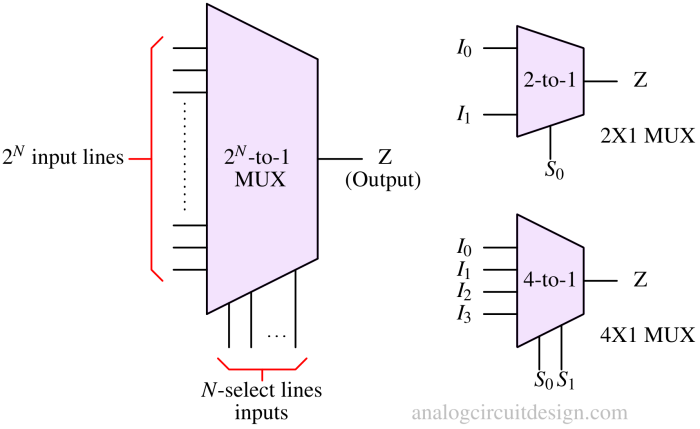
The symbol commonly used to represent a multiplexer in circuit diagrams is a trapezoid shape with multiple input lines (usually 2N lines), select lines (N), and a single output line.
Multiplexer truth table
A 2×1 multiplexer comprises two inputs, I0 and I1, one selection line, S0, and a single output, Z. When considering the selection line as an additional input, we can construct a truth table illustrating the behavior of the 2×1 MUX. The objective of the 2×1 MUX is to output I0 when S0 is zero and output I1 when S0 is one.
Below is the detailed truth table for the 2×1 multiplexer:
Table 1: Truth-Table of 2X1 Multiplexer
| S0 | I0 | I1 | Z |
|---|---|---|---|
| 0 | 0 | 0 | 0 |
| 0 | 0 | 1 | 0 |
| 0 | 1 | 0 | 1 |
| 0 | 1 | 1 | 1 |
| 1 | 0 | 0 | 0 |
| 1 | 0 | 1 | 1 |
| 1 | 1 | 0 | 0 |
| 1 | 1 | 1 | 1 |
We can observe that the truth table of a 2X1 MUX is an 8-row table. There is a way to make the table simpler as shown in Table 2. Here we will treat I0 and I1 as variables which can be assigned to Z.
Table 2 : Simplified Truth-Table of 2X1 multiplexer
| S0 | Z |
|---|---|
| 0 | I0 |
| 1 | I1 |
Similar to Table 2, we can write the truth table of a 4X1 MUX. We have four inputs I0, I1, I2, and I3 so output Z can assume any one of the input variables depending on the select line combination. To represent any one of the four inputs, we require 2 select lines that can generate four combinations.
Table 3 : Simplified Truth-Table of 4X1 multiplexer
| S0 | S1 | Z |
|---|---|---|
| 0 | 0 | I0 |
| 0 | 1 | I1 |
| 1 | 0 | I2 |
| 1 | 1 | I3 |
Multiplexer circuit diagram
The logic circuit for the 2-to-1 multiplexer can be realized using logic gates, as depicted in the Figure 2. This circuit comprises one NOT gate, two AND gates and one OR gate.

The explanation of the circuit 2X1 MUX implementation (shown in Fig 2) is following. When the select line, S0, is logic zero, the upper AND is enabled (acts like a logic buffer), while the lower AND is disabled (output of the AND is zero). Consequently, the OR gate produces an output equivalent to I0 because the other input of the OR gate is zero. Similarly, if S0 is logic 1, the upper AND gate is disabled (output is zero), while the lower AND gate is enabled and can pass I1. Hence, the output of the OR gate becomes I1.
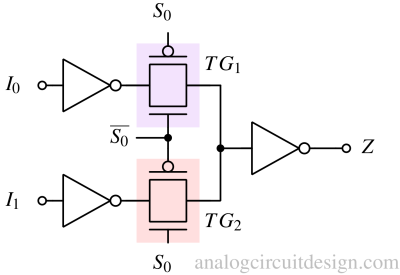
The same 2X1 MUX can be made using less number of transistors by deploying transmission gates (TG) as switches (as shown in Fig 3). When S0 is zero, the upper transmission (TG1) gate allows I0 to go through. Before Z, the I0 is inverted again to produce I0. When S0 is one, the upper transmission (TG1) gate is turned off. Instead, the lower transmission gate (TG2) allows I1 to go through. Before Z, the I1 is inverted again to produce I1.
The inverters are added to increase the input impedance and fan-out of the logic. If inverters are removed, the driver logic has to drive the load because TG doesn't supply current. TGs are just switches.
There is also a version without inverters called analog multiplexers. The version in Fig 3 can transmit only logic high or low signal. But the version shown in Fig 5 can transmit analog signals.
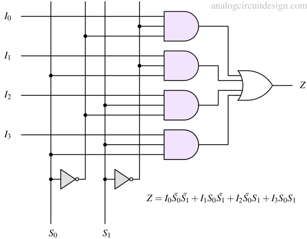
Using the above concepts, a 4-to-1 multiplexer using logic gates can be created as shown in Figure 5.
Analog multiplexer
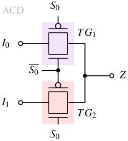
The analog multiplexer utilizes digital select lines to control the routing of analog signals as inputs. Analog multiplexers can be used as digital multiplexers too however digital multiplexers cannot be used as analog multiplexers. Analog multiplexers are made exclusively with transmission gates so that least and uniform resistance is offered throughout the signal voltages.
Multiplexer verilog code
Verilog code of a 2 X 1 multiplexer is shown below :
module mux2_1(in1, in2, select, out);
input in1, in2, select;
output out;
assign out = select ? in2 : in1;
endmodule
Basic logic gates using multiplexer
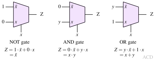
Basic logic gates can be created using a 2 X 1 multiplexer. A simple methodology can be followed to create any logic using MUX. We can write the logic function of a MUX and carefully assign the inputs. Simple examples are mentioned below :
NOT gate
To create a logic NOT function we can first write the logic function of 2 X 1 MUX:
$$Z=I_0\bar{S_0}+I_1S_0$$
Observing the above function, if we plug in I0=1 and I1=0, the output is S0. If the NOT gate we are trying to create has x as input and z as output, we can replace the select line S0 as x and obtain the output as x.
AND gate
Observing the logic function of 2 X 1 MUX we can create a logic AND function. Let's say the AND gate we are trying to create has x and y as inputs and z as output. We can plug in S0=x and I1=y in the 2 X 1 MUX logic function to create an AND gate.
OR Gate
Observing the logic function of 2 X 1 MUX we can create a logic OR function. Let's say the OR gate we are trying to create has x and y as inputs and z as output. We can plug in S0=x and I0=y, I1=1 in the 2 X 1 MUX logic function to create an OR gate.
Higher order MUX using lower order MUX
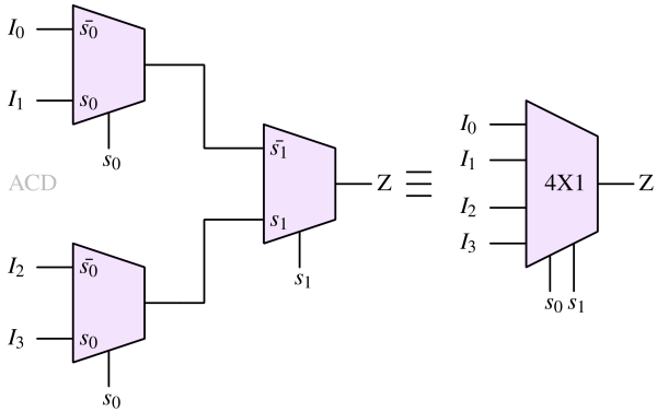
Smaller multiplexers can be used to create a single higher-order multiplexer. For instance, a 4-to-1 multiplexer can be created using three 2-to-1 multiplexers as shown in Fig 7. Two multiplexers together generate two outputs which form the input of another multiplexer. The select lines are split between the multiplexers.
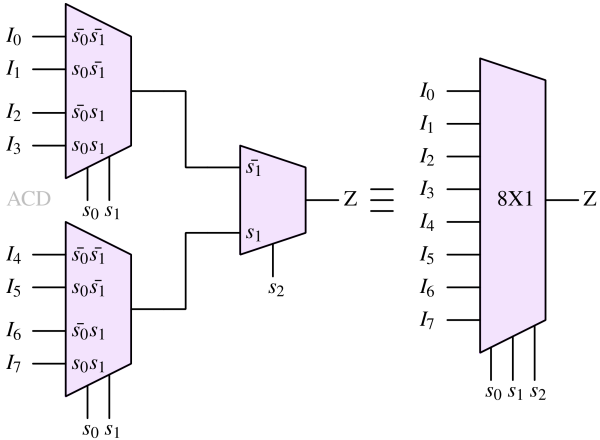 An example of 8 X 1 MUX using two 4 X 1 MUX and one 2 X 1 MUX is shown in Figure 8. s2 is the MSB of the select line while s0 is the LSB of the select line.
Multiplexer applications
- Employing a multiplexer enhances the system's efficiency by enabling the consolidation of various data types, such as audio and video, from different channels into single lines or cables for transmission.
- In computer memory, multiplexers serve to manage substantial memory capacities within computers while concurrently minimizing the number of copper lines necessary to interconnect memory modules with other components of the computer.
- Within communication networks, multiplexers play a pivotal role in combining numerous data signals onto a solitary transmission line (Time Division Multiplexing), facilitating the seamless integration and transmission of multiple calls through the network.