Non Inverting Op-Amp
In a non-inverting opamp configuration, the output voltage is in the same phase as the input voltage. The input signal is connected to the non-inverting terminal of the opamp. A part of the output signal (β.vo) is given to the inverting terminal to close the feedback loop. The main advantage of using a non-inverting opamp is that it has infinite input impedance. To compare the inverting opamp configuration, the input impedance is Ri.
 https://youtu.be/06xu3Mfdhfs
Operating principle and non-inverting opamp formula
A non-inverting opamp works on the principle of negative feedback in the presence of a large gain. To understand, let’s assume that the supply voltage is infinite.
We can analyze the operation of non-inverting op amp by considering two basic rules of ideal opamp :
- The virtual short rule: In negative feedback configuration, the inverting and non-inverting terminals have the same voltage.
- Zero input bias currents: The input terminals do not take any currents.

Assuming that the input bias currents Ibn and Ibp are zero (one of the above rules). This allows us to assume that all the current from Rf will go through Rg, and nothing will enter the op-amp's input terminals. Now, using KCL at node Vx,
$$\cfrac{V_x}{R_g}=\cfrac{V_o-V_x}{R_f}$$
$$V_o=V_x\left(1+\cfrac{R_f}{R_g}\right)$$
Using the concept of virtual short in opamp, we can assume Vx = vi,
$$V_o=V_i\left(1+\cfrac{R_f}{R_g}\right)$$
Here, Rg is the resistance from the inverting pin to the ground, and Rf is the resistance from the output to the inverting pin of the amplifier.
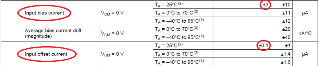
Ibn and Ibp are usually zero for CMOS (or FET) input opamps but are non-zero for BJT input opamps.
Effect of non zero input bias currents (BJT op amps)
For BJT input opamps, we start calculating the output voltage by assuming the input bias currents (Ibn and Ibp) to be zero. The input bias current causes an extra voltage at the output. So, using the superposition theorem, we can calculate the voltage caused by the bias current and add to the voltage we got when we assumed the bias current to be zero.
This extra voltage is an error that needs to be corrected. There is a very easy fix. Usually, the input bias current entering the inverting and non-inverting pins is the same. Due to a random mismatch of components inside the op amp, there is a non-zero difference, denoted by input offset current (Ios = Ibp - Ibn). We will use the superposition theorem to find the effect of Ri on the total output voltage.
Using Fig 2, we can derive the effect of Ibn on the output. We know that voltage Vx is zero due to a virtual short. We need to know the portion of Ibn's current flowing into Rf. Current through Rg is zero because the left end of Rg is connected to hard ground, and the right end is connected to virtual short. This means no voltage difference and, hence, no current. So, the entire current Ibn will flow through Rf. Therefore, the output voltage is at :
$$V_{out}=+R_fI_{bn}$$
So, the total output voltage at the output is :
$$V_o=\underbrace{V_i\left(1+\cfrac{R_f}{R_g}\right)}_{\text{Desired}}+\underbrace{R_fI_{bn}}_{\text{Undesired}}$$
A simple solution to the problem is adding an input resistor, Ri, to create an identical voltage drop, as shown in Fig 4. Now, let's find the value of Ri such that the undesired voltage at the output is zero.

Let's assume vi = 0. We can use the Superposition theorem to find the total voltage. The voltage at the non-inverting terminal (vy) of the op-amp :
$$v_y=-I_{bp}R_i$$
So, the output voltage due to the addition of Ri and the presence of Ibp is :
$$v_o=v_y\left(1+\cfrac{R_f}{R_g}\right)=-I_{bp}R_i\left(1+\cfrac{R_f}{R_g}\right)$$
Now the total voltage is :
$$V_o=\underbrace{V_i\left(1+\cfrac{R_f}{R_g}\right)}_{\text{Desired}}+\underbrace{R_fI_{bn}}_{\text{Undesired}}-\underbrace{I_{bp}R_i\left(1+\cfrac{R_f}{R_g}\right)}_{\text{Correction}}$$
The correction term should cancel the undesired term completely. So,
$$\underbrace{R_fI_{bn}}_{\text{Undesired}}-\underbrace{I_{bp}R_i\left(1+\cfrac{R_f}{R_g}\right)}_{\text{Correction}}=0$$
Assuming Ibn = Ibp, we get :
$$R_i=\cfrac{R_fR_g}{R_f+R_g}=R_f||R_g$$
So, to cancel the effect of input bias currents in an op-amp, a resistor Ri is added which is parallel combination of Rf and Rg.
Buffer opamp (voltage follower)

In the case of a non-inverting opamp configuration, a buffer (op amp with gain = +1 V/V) can be made by keeping Rf = 0. The main purpose of buffer opamp is to isolate the signal from the load. That means it does not allow the signal to flow from output to input but allows the signal to flow from input to output. Isolation is provided because the input impedance of the buffer is very high (> 1MΩ), and the output impedance is very low (<10Ω).
If the input impedance is high, it does not demand current from the signal source. If the output impedance is very low, it can provide the necessary current to maintain the output voltage without a significant voltage drop at the output.
Buffers are used in instrumentation amplifiers to make the input impedance very high. Also, a diode can be inserted in the output to make a precision rectifier.
Properties of non-inverting opamp
- Infinite input impedance (or limited by opamp's input impedance which is usually high).
- Positive gain (>= 1 V/V).
- Output impedance same as inverting opamp configuration.
Real opamp requirements
To operate an opamp in non-inverting opamp, the allowed input voltage swing should be high. For example, For a supply voltage of ±5V, if the input signal is 8Vpp (or ±4Vp), the common mode range supported should be atleast ±4Vp.

Look out for the common mode input range of the opamp in the datasheet. For e.g., in the above figure, for a supply voltage of ±5V, the maximum input swing is ±3.8V, which is not sufficient of 8Vpp. Below we can see an opamp which can support ±4Vp on ±5V supply:

In the above figure we can see that the amplifier is responsive till 0.2V above and below the highest and lowest supply voltage. These are called rail-to-rail input operational amplifier. This is suitable for our requirement of ±4V input range requirement.
Distortion of non-inverting operational amplifier
Since the input stage is moving with the input signal, the input stage sees a large voltage swing across it. This leads to higher distortion in non-inverting amplifier in comparison to an inverting amplifier. In inverting amplifier configuration, the input stage is not moving because it is virtually shorted to ground.
Stability of non-inverting amplifier

The parasitic input capacitor (Cpar) can form an undesirable pole with sufficient high Rf||Rg. This pole appears before the amplifier's gain-bandwidth product, which results in a degraded phase margin. To solve the problem, we can do the following things:
- We can reduce the value of Rf to increase the pole frequency. This will require an op-amp to drive the new Rf (a high-current drive capability op-amp).
- We shunt the Rf with a capacitor Cf to introduce a zero after the pole and before the gain bandwidth. This restores the opamp's phase margin in negative feedback. The value of Cf has to be chosen so as not to increase the rise time while improving the phase margin.
- Sometimes, the value of Cpar is very small (~ pF), so getting those small capacitors could be tough. This makes us use a higher value of capacitances, leading to a sluggish output waveform. A capacitor (Cg) parallel with Rg can be added to improve that. This method improves the stability and maintains a fast rise time. We must ensure the amplifier is stable at CgCf/(Cg+Cf) capacitance.