Opamp offset voltage and current
Offset voltage in opamp is a small non-ideal voltage difference between inverting and non-inverting pin of the opamp in closed loop. Ideally, this voltage difference should be zero.
Another way of looking at the opamps offset voltage - If both inputs of opamp is shorted together, the output should also be zero as per the related shown below :
$$V_{out}=A(V_{ip}-V_{im})$$
In reality, the op-amp output saturates to one of the supply rails if both inputs are connected together because of this op-amp offset. The output voltage is the op-amp's gain times the offset voltage, which often results in a value larger than the supply voltage.
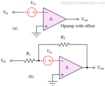
Sources of opamp's offset
The offset is caused by manufacturing process variations, and random mismatch (asymmetry).
In CMOS opamps, a major offset contributor is the Vth mismatch in the input stage. The Vth is a function of doping levels, the thickness of gate oxide, etc.
Offset cancellation applications
In applications like sensor reading, the signal voltage change could be very low. It may be in the range of <100μV. This small voltage needs to be amplified to an ADC readable value. To do that, it is amplified using an opamp (having an offset of 1 mV) with a gain of 1000 V/V. The expected output of the opamp is 0.1V. However, the output is coming to be 1.1V.
This is because the gain is amplifying the offset too. The amplifier's offset is 1mV; when multiplied by 1000 V/V, it gets to 1 V. Over and above it, we have an amplified sensor value.
Offset voltage cancellation techniques
There are primarily two ways to cancel offset in an opamp which are mentioned below:
Static offset cancellation
In this offset cancellation, the circuit change is made once during production after measuring the offset. No change is made while the chip is operational. There are two major static offset cancellation techniques :
Dynamic offset cancellation
While static offset cancellation is done once during production, dynamic offset cancellation is done repeatedly during the operation of the opamp. There are two well-known dynamic offset cancellation techniques :
Trimming
Trimming involves measuring and then reducing the offset using some permanent change in the circuit. This is done once during production or testing. This can reduce the offset by order of magnitudes.
Resistor-based trim
The offset is measured, and one particular resistor (designed to change offset) is physically cut (using a laser) inside the IC to get the desired offset.
Current source-based trim
The offset is measured, and some current sources are added or removed to get the desired offset level.
The main advantage of trimming is that it can support high-speed applications (> 1 MHz), which dynamic offset cancellation techniques cannot support.
Trimming is usually done for a single temperature, which does not solve the offset drift (with temperature). Therefore, multi-temperature might be required to cancel the drift. Trimming cannot remove flicker noise.
For low-frequency applications (< 1 MHz), trimming cannot provide the level of offset and drift performance as chopping. So, for sensor applications (usually slow ~ 1-100 Hz), opamps with chopping are preferred over trimmed opamps.
Calibration
Calibration is like measuring the error due to offset once and removing that error value each time while making an actual sensor reading. However, we need to do calibration repeatedly with changing conditions because the offset changes with conditions like temperature, humidity, pressure, etc.
Auto-zeroing
In the Auto Zero technique, the offset voltage is stored in a capacitor in phase 1. Phase 1 is the time when the signal is not allowed to flow and it is solely used to capture the inherent offset of the op-amp. In Phase 2, the offset captured in the capacitor is added/subtracted to the signal voltage. This makes sure that the output has only a signal and no offset.
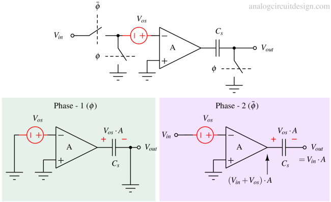
The above figure shows a general scheme of auto-zero amplifiers. The operation is divided into two phases: Phase 1 and Phase 2. At the top, the offset voltage is denoted using a fixed voltage source (Vos). In phase 1, we connect the left side of the voltage source to the ground. It results in an amplified offset of Vos times A, which appears at the output of the amplifier. The switch of output is also connected to the ground in phase 1. Therefore, the capacitor is charged to VosA voltage.
In the next phase, phase 2, the Vin is connected directly to the left side of the Vos, and the previous connection to the ground is opened. At the same time, the capacitor's connection to the ground at the output is also opened. Now, the amplifier's output is (Vin+Vos)A. However, the final output would be subtracting the voltage stored in the capacitor, which is VosA. So, the final output is VinA. Hence, the offset voltage is removed.
The scheme mentioned in Fig 2 has a problem. The offset voltage could be a few mV, and the opamp's gain could be 105 V/V. This will cause the output to saturate to the supply voltage, which may not be high enough to accommodate the VosA voltage.
For example, if the Vos = 1mV and A=105 V/V, the expected output voltage would be 100V. If the supply voltages (VCC and VEE) are +-5V, the output would be saturated to +-5V. So, this saturated voltage would be stored in the capacitor during phase 1. Ideally, it should have stored 100V across the capacitor during phase 1. So, the above scheme won't work in real scenarios and needs some modifications.
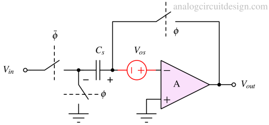
The scheme mentioned in Fig 3 deals with the problem of saturation at the output. In phase 1, the offset value will be directly stored in the capacitor. This is because, in phase 1, the amplifier's output equals -Vos (in unity gain configuration or buffer). The capacitor's right plate is connected to -Vos and the left is connected to the ground. So, the capacitor is charged to -Vos. In Phase 2, the capacitor is connected in series with the offset voltage. This cancels the Vos, and the output completely depends on Vin instead of Vin+Vos.
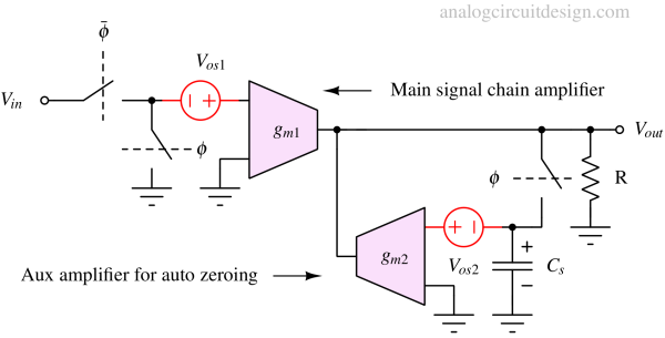
Chopping
Chopping is a common technique for reducing the amplifier's offset voltage, offset voltage drift over temperature and flicker noise. In summary, it removes all low-frequency components to a higher-frequency component and attenuates using a low-pass filter, as shown in Fig 5.
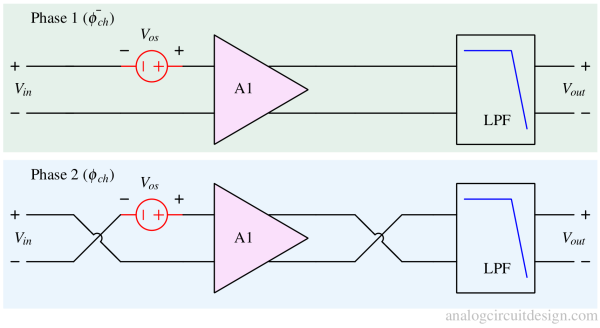
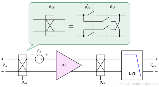
In a chopper amplifier, two sets of switches are present. One is at the input stage, and another is at the output stage of the opamp. Each switch's function is to interchange the two input lines (vip and vim). As shown in Fig 5, in phase 1, vip is connected directly to the offset source. This results in VosA offset at the output. In phase 2, the vim is connected directly to the offset source. At the same time, to maintain negative feedback for the outer loop, the output is also crossed. This results in an output offset voltage of -VosA.
The switching between phase 1 and phase 2 happens rapidly with the help of a clock signal. Therefore, a DC offset appears as an AC voltage with an average zero value in the time domain. The output has an AC signal with an amplitude of VosA. This AC signal is attenuated using a low pass filter.
Issues with dynamic offset cancellation techniques
There are several advantages of dynamic offset cancellation over static offset cancellation, such as no additional test cost overhead, the offset performance won't degrade with device aging/healing, and reducing 1/f noise.
However, there are some issues which are there in dynamic offset cancellation. These can be minimized with careful circuit techniques:
Charge injection and Clock feedthrough
Clock feedthrough is defined as the amount of clock frequency appearing at the amplifier's output. It happens due to parasitic capacitances injecting charges into sensitive nodes, such as the amplifier's input.
Ripples
Ripples are the time domain unwanted waveforms appearing at the output of the amplifier at the chopping frequency. Ripples appear because of charge injection.
Many chopper amplifiers have ripple rejection filters built inside them. The ripple rejection filter uses a notch filter or a low-pass filter in the feedback to suppress the ripples appearing at the notch frequency.
Lesser bandwidth
The bandwidth of chopper amplifiers is usually lower than that of their non-chopper counterparts. This is because the amplifier's gain bandwidth product is lower than the chopping frequency.