Photodiodes
A photodiode is a p-n junction diode that responds with a change in current whenever photons with sufficient wavelength hit the depletion region. To get the depletion region, it is usually operated in reverse bias. It can be called a transducer which can convert light energy into electrical energy. The current level are proportional to number of photons (i.e., intensity of light). Some applications are - remote control, spectroscopy, isolation, laser range finder, sensors, optical communications etc.
Behaviour of electron-hole pairs in depletion region.
Using a thought experiment, let's try to understand what happens if somehow an electron-hole pair is placed in the depletion region. Depletion region is generated if n-type region is connected to more positive voltage than p-type region (i.e., reverse bias mode). So, electron will be attracted towards the n-type region. Similarly the hole will be attracted towards p-type region. So, a fact is established that if somehow an electron-hole pair is generated in the depletion region, the charge carriers will drift to the opposite potential terminals.
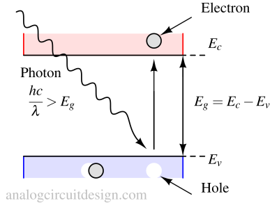
A hole is generated in the valence band as soon as electron jumps to conduction band. That is why it is called electron-hole pair. During recombination, electrons from the conduction band occupies the hole in the valence band.
Photoconductive effect

Whenever a photon with energy equal to the bandgap hits the depletion region, an electron jumps to the conduction band. In short electron-hole pair is generated. Any p-n junction, if illuminated with light of sufficient wavelength is a potential photodiode. To allow light to enter the p-n junction, a transparent window is provided.
Construction of Photodiode

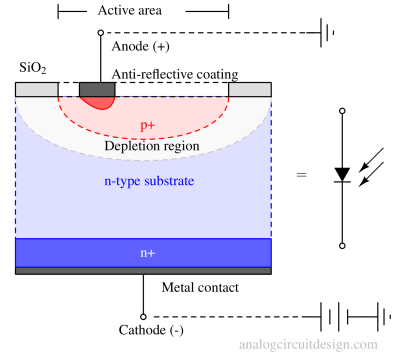
The construction is similar to that of a regular p-n junction diode. However, special care has been taken to allow light to pass into the depletion region.
How to connect photodiode ?
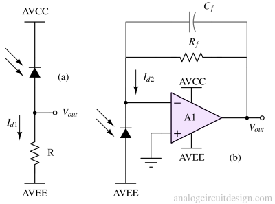
Photodiodes are usually operated in reverse bias mode. If operated in forward bias mode, the photocurrent will be very less in comparison to the diffusion current. For high-speed operating, the reverse bias voltage should be large so that the junction capacitance becomes low. This is due to depletion region widening. In Fig. 3(a), the circuit is not well optimized for high-speed operation (>10MHz) because of the high resistance value of R (with junction capacitance, it becomes a low-pass filter). Fig. 3(b), is optimized for high speed and moderate gain. (Cf) is added for the high-frequency stability of the amplifier.

Small signal model of photodiode

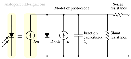
A photodiode can be modeled as a diode in parallel with IPD (Photo-Diode current), ID (dark current), Cj (Junction capacitance), Shunt resistance, and Series resistance. These components define the AC and DC response of the photodiode in simulation.
What are the noise sources in a photodiode ?
Major noise sources in a photodiode can be categorized as thermal noise, shot noise, and dark current noise.
Junction capacitance
The junction capacitance of a photodiode, often referred to as the photodiode capacitance, is an important parameter that characterizes the photodiode's response to changes in light intensity. It plays a crucial role in determining the photodiode's bandwidth or response time.
Depletion region capacitance
Usually, a photodiode is reversed-biased. When no light is incident on it, there is a depletion region at the p-n junction. This depletion region is devoid of free charge carriers (electrons and holes) and acts like a dielectric between the p-type and n-type semiconductor regions. The depletion region capacitance is formed due to the separation of charge carriers on either side of the junction. The bandwidth (speed) of a photodiode is inversely proportional to the junction capacitance. A lower junction capacitance allows the photodiode to respond to higher-frequency variations in light intensity. This is particularly important in applications that require fast detection of light fluctuations, such as optical communication systems.
What is dark current in photodiode ?
Dark current refers to the small measurable current that flows through the photodiode even when there is no incident light (darkness). It is also known as leakage current or reverse bias current. Dark current is an intrinsic characteristic of photodiodes and is caused by several factors:
- Thermal Generation: One of the primary contributors to dark current is the thermal generation of electron-hole pairs within the photodiode's semiconductor material. At higher temperatures, thermal energy can create electron-hole pairs even in the absence of incident photons. This phenomenon increases the dark current.
- Recombination: In a photodiode, electrons, and holes are generated due to thermal energy, and some of them recombine, creating a small but nonzero current. The rate of recombination is temperature-dependent.
- Defects and Impurities: Impurities and defects in the semiconductor material can also contribute to dark current by allowing charge carriers to move more freely than they would in a perfect crystal lattice.
- Reverse Bias: Dark current is more pronounced in photodiodes operated in reverse bias mode, where a reverse voltage is applied across the p-n junction. This bias voltage can enhance the flow of dark current, especially in avalanche photodiodes (APDs), which are designed for high sensitivity.
What is responsivity of photodiode?
Responsivity: Quantum efficiency is related to the photodiode's responsivity (Rλ), which is the ratio of the photocurrent Ip (A/m2) to the incident optical power P (W/m2). Responsivity can be expressed as:
$$R_{\lambda{}}=\cfrac{I_p}{P} (A/W)$$
What is quantum efficiency in photodiode ?
Quantum efficiency (QE) is the ratio of the number of electron-hole pairs generated by the incident photons to the total number of incident photons. High quantum efficiency is desirable in photodiodes because it means that a larger fraction of incident photons are converted into electrical current, resulting in better sensitivity and SNR (signal-to-noise ratio). Quantum efficiency is expressed as a percentage or a fraction and it is a dimensionless quantitiy.
Mathematical Representation: Quantum efficiency is often denoted by the symbol "η" (\eta) and is calculated using the formula:
$$\eta{}=\cfrac{\text{Number of electrons collected}(r_e)}{\text{Number of incident photons}(r_p)}$$
Peak QE: Photodiodes often have a peak quantum efficiency at a specific wavelength where their sensitivity is highest. The peak QE wavelength depends on the material used in the photodiode. For example, silicon photodiodes typically have peak QE in the visible or near-infrared range.
Relation between quantum efficiency and responsivity
$$R_{\lambda{}}=\cfrac{I_p}{P}$$
$$P=r_p\cdot{}h\cfrac{c}{\lambda{}}$$
rp is the rate of photon incident on the surface of the material. hc/λ is the energy per photon. From the Quantum efficiency relation, we get:
$$r_e=\eta{}\cdot{}r_p$$
η is the quantum efficiency. Substituting the relation of re and P in Rλ, we get:
$$I_p=e\cdot{}r_e$$
$$I_p=e\cdot{}\eta{}\cdot{}r_p$$
$$R_{\lambda{}}=\cfrac{e\cdot{}\eta{}\cdot{}r_p}{r_p\cdot{}h\cfrac{c}{\lambda{}}}=\cfrac{e\cdot{}\lambda{}\cdot{}\eta{}}{h\cdot{}c}$$
$$R_{\lambda{}}=\cfrac{\eta{}\lambda{}}{1.24}$$
What is photovoltaic mode in photodiode ?
Photovoltaic mode refers to the operating mode of a photodiode or photodetector where the device is used as a photovoltaic cell or solar cell to directly convert incident light or photons into electrical energy or voltage. In this mode, the photodiode generates a voltage across its terminals when exposed to light, without any external bias applied to it.
Photons from incident light are absorbed by the semiconductor material of the photodiode, creating electron-hole pairs. These generated electron-hole pairs are separated within the photodiode, creating an internal electric field. This electric field causes charge carriers (electrons and holes) to move, resulting in a voltage difference across the photodiode terminals.