Pipeline ADC
A pipeline ADC (Analog-to-Digital Converter) is a type of ADC that divides the conversion process into multiple stages, each of which contributes a portion of the final digital output. In a pipeline ADC, the input signal goes through a sequence of stages, each performing a partial conversion, and then these partial results are combined to produce the final digital output.
This architecture is designed to achieve high-speed and high-resolution analog-to-digital conversion using the concept of parallelism and time-interleaving. In parallelism, multiple stages process the input data concurrently, and in time-interleaving, each stage handles a different part of the input signal in time domain. This approach allows pipeline ADCs to achieve high throughput. It is commonly used in applications requiring rapid conversion of analog signals into digital form, such as in communication systems and instrumentation.

Architecture and components of Pipeline ADC
Some common sub-blocks of a pipeline ADC are:
Sample and Hold
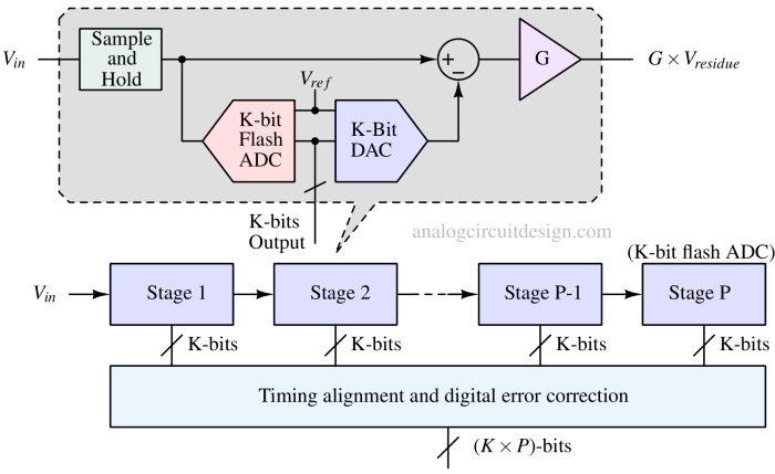
Every stage requires a sample-and-hold (S/H) function. During the tracking phase, it acquires the input/residue from the previous stage. In the holding phase, sub-ADC makes the conversions and computes the residue.
K-bit flash ADC
Flash ADCs are used to convert rapidly from analog to digital signal. Usage of Flash ADCs avoids the timing complications associated with other architectures. Usually 2-bit or 3-bit flash ADCs are used. So, each stage can give out 2-3 bits of digital data at a time.
K-bit DAC
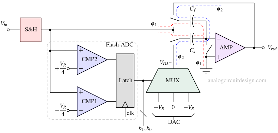
A rapid conversion DAC is used to convert the quantised data into analog data. This analog data is what is perceived by the ADC and now will be used to find the residue. Most of the time, it is MUX based design so that it is fast and occupies less area. One example is shown in Fig 2.
Residue generator
This circuit takes the difference between the signal sampled by the S/H block and K-bit DAC to produce residue for the next stage in the pipeline.
Working of a pipeline ADC
As shown in the Fig 1, the analog input, Vin goes through a series of stages. Each stage is an ADC, so it should convert an incoming analog signal into digital bits. Also, each stage should generate the residue to be used by the next stage. So a DAC is used to convert the digital signal into analog which is quantised. Now a difference is taken between actual analog and quantised analog to create the residue. This residue is then amplified so that the Flash ADC’s comparators in the next stages resolve the signal easily. Now it is no longer necessary to scale down Vref in next stages. Also, the accuracy requirements for stages following stage 1 are reduced.
This amplified residue travels through the pipeline, contributing K-bits per stage, until it reaches the final stage, which is a K-bit flash ADC alone resolving the last K least significant bits (LSB). Since each stage determines its bits at different points in time, all the bits corresponding to the same sample are aligned in time using shift registers before being processed by the digital error-correction logic.
Single stage design
In the realm of high-speed CMOS pipelined ADCs, there's a tendency to opt for a lower number of bits per stage, sometimes as minimal as just one bit per stage. This choice ensures that the interstage gain remains modest, typically around a factor of 2. The rationale behind this decision lies in the inherent challenges of designing wideband amplifiers with exceptionally high gain in CMOS technology.
On the other hand, when it comes to lower sampling-rate CMOS pipelined ADCs and even high-sampling-rate bipolar pipelined ADCs, there's a preference for incorporating more bits per stage. This approach not only enhances the ADC's resolution but also reduces data latency, making it a pragmatic choice for various applications.

This section delves into the well-known 1.5-bit-per-stage architecture (shown in Fig 2). In this configuration, each stage is responsible for resolving one bit, with 0.5-bit overlap. Specifically, each 1.5-bit stage employs a 1.5-bit flash ADC, featuring only two comparators, as opposed to a complete 2-bit flash ADC.
In Phase-1 (φ1), Both Cf and Cs are charged to Vin, as both are connected to Vin and Ground. In Phase-2 (φ2), Cs is connected to VDAC and virtual ground of the opamp, and Cf is connected to output and virtual ground of the opamp. To charge Cs to VDAC, (VDAC - Vin)Cs charge moves to discharge Cf (discharge because the difference charge moving into Cf through bottom plate). So, total charge remaining in Cf is VinCf - (VDAC - Vin)Cs. Therefore, the voltage of the top plate of Cf is (also happens to be residue voltage Vrsd):
$$V_{rsd}=\cfrac{V_{in}C_f-(V_{DAC}-V_{in})C_s}{C_f}$$
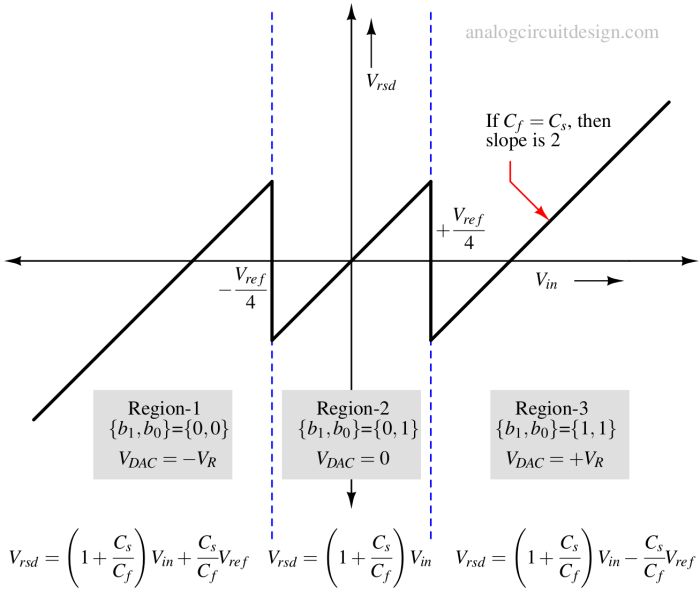
$$V_{rsd}=V_{in}\left(1+\cfrac{C_s}{C_f}\right)-V_{DAC}\cfrac{C_s}{C_f}$$
The value of VDAC changes with Vin because VDAC is generated through a cascade of ADC and DAC. So, let's plot VDAC and Vin characteristics:

Application of pipeline ADC
The pipelined analog-to-digital converter (ADC) has emerged as the predominant ADC architecture for sampling rates spanning from a few mega samples per second (Msps) to speeds exceeding 100Msps. It offers resolutions starting at eight bits for the higher sample rates and extending up to 16 bits for the lower rates. This diverse range of resolutions and sampling rates accommodates a wide spectrum of applications:
- CCD imaging
- Ultrasonic medical imaging
- Digital video applications (such as HDTV)
- xDSL
- Cable modems
- High-speed Ethernet.