PN junction diode
A p-n junction is a combination of two types of semiconductor materials, p-type and n-type, in a single semiconductor substrate. The n-type side contains freely moving electrons, while the p-type side contains freely moving electron holes. P N junctions are used to create transistors, diodes, and isolation between transistors. Understanding the P N junction goes a long way toward understanding semiconductor device physics (e.g., LEDs).

What is a diode?
A diode is an electrical device that allows current to flow only in one direction. Ideally, it offers zero resistance in one direction, which allows current to flow, and infinite resistance in the reverse direction. Most of the diodes in electronics are based on PN junctions.
P N junction diode definition
A PN junction can act as a diode. It allows current to flow when the p-type side of the PN junction is at a higher voltage than the n-type side (also called forward bias condition). It does not allow current to flow when the p-type side is at a lower voltage than the n-type side.
P N junction diode symbol

The symbol for a p-n junction diode typically looks like this: The triangle (arrowhead) points towards the direction of current flow. The vertical line is the n-type side, and the triangle portion represents the p-type side.
What is anode and cathode of a diode?
In a PN junction diode, the terms “anode” and “cathode” refer to the two terminals of the diode.
- Anode: The anode is the diode’s positive (+) terminal. The P-type semiconductor is associated with the anode in a PN junction diode. It is where the holes, which are positive charge carriers, are prevalent.
- Cathode: The cathode is the diode’s negative (-) terminal. The N-type semiconductor is associated with the cathode in a PN junction diode. It is where the electrons, which are negative charge carriers, are prevalent.

Construction of P N junction diode
The most common way to create a PN junction is by implanting or diffusing donors (pentavalent atoms like Phosphorus or Arsenic) into a P-type substrate such that a semiconductor layer is converted into an N-type. Converting an N-type semiconductor layer into a P-type with acceptors (trivalent atoms like boron) would also create a PN junction.

Working principle of P N junction diode
When a P N junction is forward-biased, the built-in barrier voltage is reduced, causing thermally generated mobile carriers (electrons) to diffuse across the depletion region. This diffusion is substantial when the forward voltage is near or above 0.7V, causing a large amount of current to flow. In reverse bias, the diffusion is inhibited, and only the drift current exits. The drift current is minimal (~nA). So, in reverse bias, the P N junction appears to be non-conductive.
Types of current in P N junction
When the PN junction is in forward bias, diffusion current dominates the total current. When the PN junction is in reverse bias, the current is dominated by drift current. In zero bias, the drift current equals diffusion current, hence zero total current. The differences between drift and diffusion current are mentioned below :

Diffusion current
The motion of charge carriers from higher concentration to lower concentration causes a current called diffusion current. In a semiconductor with n-type and p-type sides, the n-side has more electrons, and the p-side has more holes, forming concentration gradients. This causes electrons to flow from the n-type to the p-type side and holes to move in the opposite direction, resulting in a current from the p-type to the n-type side.
Drift current
Drift current is the electric current generated by particles moving under the influence of an electric field. This field arises either from an applied external voltage or a depletion region. With an external voltage, the field directs from the positive to the negative terminal, causing electrons to move toward the positive terminal and holes toward the negative. In the depletion region’s field, electrons drift toward positively charged donor atoms, while holes move toward negatively charged acceptor atoms.
Current-voltage relationship of P-N Junction Diode
When a P N junction has zero bias (no external voltage), the potential barrier prevents current flow. In forward bias, the potential barrier is reduced, allowing current to flow. For silicon diodes, this reduction occurs at 0.7V. Below 0.7V, the current is very low. The following figure shows the IV characteristics of the PN junction diode:
$$I=I_s\left(e^{qV/kT}-1\right)$$

In reverse bias, a slight reverse saturation current (~nA) flows due to thermally generated electron-hole pairs in the depletion region being swept away by the applied reverse bias voltage. The junction breaks down beyond a specific reverse bias voltage and a huge current flows.
Biasing Conditions for the P-N Junction Diode
There are three biasing conditions for the P-N junction diode, and this is based on the voltage applied on the terminals:
- No bias or Zero bias: No external voltage is applied to the P-N junction diode.
- Forward bias: The external voltage applied is such that the P-type potential is higher than the N-type potential. In other words, the P-type voltage is positive, and the N-type voltage is negative.
- Reverse bias: The external voltage applied is such that the P-type potential is lower than the N-type potential. In other words, the P-type voltage is negative, and the N-type voltage is positive.
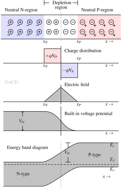
No bias PN junction
No-bias or Zero-bias is a condition when no voltage is applied across the junction. The junction can be divided into three regions: neutral p-region (x > xp), neutral n-region (x < -xn), and depletion region in between (-xn < x < xp).
Formation of the depletion region
When P-type and N-type regions are created side by side, they form a depletion region. Upon contact, free electrons from the n-type region diffuse into the p-type region, while free holes from the p-type region diffuse into the n-type region. As a result, a region around the junction becomes depleted of mobile charge carriers (electrons and holes) and uncovers immobile charges. This area is called the depletion region.
The charge density is zero everywhere except in the depletion layer, where it is equal to the dopant charge density. From region 0 < x < xp , charge density n=NA . For region -xn < x < 0 , charge density p=ND.

Built-in potential (Threshold voltage)
In this depleted region, only fixed, immobile ions remain: negatively charged acceptor ions on the p-type side and positively charged donor ions on the n-type side. This creates an electric field across the junction, which opposes further movement of charge carriers and establishes a potential barrier, preventing additional diffusion and recombination of electrons and holes across the junction. This means that charge carriers need additional energy to move from the depletion region's nearest edge to its opposite end. This extra work per charge is called built-in potential.
The barrier potential can be derived using the difference between quasi-Fermi (Efn, Efp) and intrinsic-Fermi (Efi) levels (shown in Fig 7).
$$V_{bi}=(E_{fn}-E_{fi})+(E_{fi}-E_{p})$$
$$\implies{}V_{bi}=\cfrac{kT}{q}ln{\left(\cfrac{N_D}{n_i}\right)}+\cfrac{kT}{q}ln{\left(\cfrac{N_A}{n_i}\right)}$$
$$\implies{}V_{bi}=\cfrac{kT}{q}ln{\left(\cfrac{N_D\cdot{}N_A}{n_i}\right)}$$
Threshold voltage of some PN junction diodes
| Diode Type | Forward Threshold Voltage |
|---|---|
| Silicon Schottky | 0.15V - 0.45V |
| Germanium PN | 0.25V - 0.3V |
| Silicon PN | 0.6V - 0.7V |
| Red LED (GaAsP) | 2V |
| Green LED (GaP) | 2.2V |
| Blue LED (InGaN) | 3.5V |
Width of depletion region
The width of the depletion region is inversely proportional to dopant density. The depletion region is very narrow if the dopant density is very high. If the dopant density is low, the depletion region is wide.
$$W_{dep}=\sqrt{\cfrac{2\epsilon_sV_{bi}}{q}\left(\cfrac{1}{N_A}+\cfrac{1}{N_D}\right)}$$
Let's assume that the equilibrium has reached and the depletion region is formed. Now, the built-in potential would be the energy required per charge to push the electrons from (x = -xN) to (x = +xP). This pushing force is nothing but thermal agitation.
The electric field in the depletion region -xN<x<+xP:
$$\vec{E} = -\cfrac{qN_D(x_P-x)}{\epsilon{}}, 0<x<x_N$$
$$\vec{E} = -\cfrac{qN_A(x_N+x)}{\epsilon{}}, -x_N<x<0$$
Electric field outside the depletion region will be 0, because there is 0 net charge enclosed by gaussian surface. Work done (W) by thermal energy to push a electron from +xP to -xN.
$$W = \int_{-x_N}^{x_P}(-q).\vec{E}.\vec{dx}$$
$$\therefore{} W = \cfrac{q^2}{2\epsilon{}}\left(N_Ax_N^2+N_Dx_P^2\right)$$
So, work done by a unit positive charge (also potential),
$$V_{bi} = \cfrac{W}{q} = \cfrac{q}{2\epsilon{}}\left(N_Ax_N^2+N_Dx_P^2\right)$$
Where, $$q = +1.6\times{}10^{-19},\text{C}$$
From charge neutrality in the depletion region,
$$N_Dx_P = N_Ax_N$$
Let's assume, (Wdep = xP + xN). From the above equations,
$$V_{bi} = \cfrac{qW_{dep}^2}{2\epsilon{}}\cfrac{N_AN_D}{N_A+N_D}$$
$$W_{dep} = \sqrt{\cfrac{2\epsilon{}V_{bi}}{q}\left(\cfrac{1}{N_A}+\cfrac{1}{N_D}\right)}$$
Forward Biased PN junction
When the P region has a higher potential than the N region, the PN junction is said to be forward-biased.

Minority carrier injection
A forward bias voltage (VF) reduces the barrier height from φbi to φbi – VF. This reduces the drift field, which was balancing the diffusion current during zero bias. Electrons can now diffuse from the N side into the P side. Similarly, holes are injected from the P side into the N side. This is called minority carrier injection. The word “minority” is used because the electrons diffuse into the P region, where it is the minority carrier.
We can visualize the effect by assuming the barrier is some floodgate in a river dam. When the floodgate is lowered (using external forward bias voltage), the water (mobile carriers) rushes through the gates.
Excess minority concentration
The external forward voltage causes an increase in minority carrier concentration at the edge of the depletion region by a factor of eqV/kT. So, after the forward bias, the minority carrier concentration is n0eqV/kT, where n0 was the minority carrier concentration when no forward bias was applied (i.e., zero bias). So, the excess minority carrier concentration is :
$$n'=n_0e^{qV/kT}-n_0=n_0\left(e^{qV/kT}-1\right)$$
Stored charge
When a PN junction diode is forward-biased, the excess electrons and holes are called stored charges. The stored charge is proportional to the current (ID).
$$Q=I.tau{}_s$$

This storage charge contributes to the small signal capacitance called diffusion capacitance.
Total current of diode
The total current of a P N Junction diode can be represented using the following mathematical expression. This equation covers both forward and reverse bias regions. However, it does predict the diode's avalanche breakdown.
$$I=I_s\left(e^{qV/kT}-1\right)$$
$$I_s=A\cdot{}q\cdot{}n_i^2\left(\cfrac{D_p}{L_pN_D}+\cfrac{D_n}{L_nN_A}\right)$$
It is called reverse saturation current. “A” is the diode's cross-section area. “q” is the unit charge, having a value of 1.6 x 10⁻¹⁹C. ni is the intrinsic carrier concentration. ni’s dependence on fundamental quantities is mentioned below:
$$n_i^2=4\left(\cfrac{2pi{}kT}{h^2}\right)^3(m_e^*m_h^*)^{3/2}e^{-E_g/kT}$$
Eg = Ec - Ev is called bandgap energy. Since ni2 is proportional to T3, the reverse saturation current has a very strong temperature dependence.
Reverse bias PN junction
When the P region has a lower potential than the N region, the PN junction is said to be reverse-biased.
In reverse bias, the mobile charge carriers don’t diffuse because they are attracted toward the opposite polarity potential. For instance, electrons from the N region move toward the battery's positive terminal. In contrast, holes in the P region move toward the battery's negative terminal, as shown in the following figure. Consequently, the depletion region width increases.

Electric field in a reverse-biased junction
The electric field can be mathematically represented as : $$overrightarrow{E}=\cfrac{V}{d}=\cfrac{V_r}{\sqrt{2\epsilon{}(phi{}+V_r)/qN}}\simeq{}\sqrt{(qN/2\epsilon{})V_r}$$ $$\implies{}|\overrightarrow{E}|\propto{}\sqrt{V_r}$$ The electric field across the depletion width is proportional to the square root of the applied reverse bias.
Junction breakdown of diode in reverse bias
Junction breakdown refers to the phenomenon of the current abruptly increasing when reaching a critical reverse bias voltage. Junction breakdown is not inherently destructive. As long as an external circuit keeps the current within a reasonable limit, preventing excessive heat dissipation in the PN junction, it can safely operate in reverse breakdown mode.
There are the following types of junction breakdown :
- Avalanche breakdown (due to impact ionization)
- Zener breakdown (due to tunneling)
Let’s understand the avalanche breakdown in this article. As the electric field increases, electrons moving through the depletion layer gain more kinetic energy. Some of these electrons acquire enough energy to excite an electron from the valence band to the conduction band, generating an electron-hole pair. This process is known as impact ionization. The electric field further accelerates the newly created electrons and holes, enabling them and the original carriers to generate even more carriers through impact ionization. This chain reaction resembles a snow avalanche, which is why it is called avalanche breakdown.
Depletion capacitance
The depletion layer and the neutral N and P regions may be viewed as dielectric (insulator) sandwiched between two conductors. Therefore, the PN junction may be modeled as a
parallel-plate capacitor with capacitance :
$$C_{dep}=A\cfrac{\epsilon{}_s}{W_{dep}}$$
Small signal model of diode
It is very common in analog circuits to use a diode with a constant DC bias in a signal path. The diode is forward-biased in this situation because it allows current to flow.

Small signal resistance of a diode
Ideally, the diode should offer zero resistance for small changes in voltage. However, it introduces a resistance (rd).
$$V_d=V_t\cdot{}ln{\left(I_d/I_s\right)}$$
$$r_d=\cfrac{dV_d}{dI_d}=V_t/I_d$$
Where Vt = kT/q and Is = reverse saturation current.
Small signal capacitance of a diode
The small signal capacitance of the diode consists of two components :
- Diffusion capacitance
- Depletion capacitance
Diffusion capacitance :
This capacitance is called diffusion capacitance because it occurs due to the forward-biased diffusion current.
$$C=\cfrac{dQ}{dV}=tau{}_s\cdot{}dI_d/dV_d=tau{}_s/(dV_d/dI_d)=tau{}_s/r_d$$
Depletion capacitance
In the forward bias condition, it may seem that Wdep approaches zero, and as a result, Cdep approaches infinite. It should be noted that, when Wdep approaches zero, the depletion charges also approaches zero. Therefore, Cdep saturates to 2-3 times Cdep at zero bias.
P N junction diode temperature effect
Higher temperatures lead to more covalent bond breakage, increasing intrinsic charge carriers (ni). The dependence of ni with temperature is extreme (ni ∝ T3). This results in a very high reverse saturation current (Is). This phenomenon affects both forward and reverse currents. In forward bias, the IV (current-voltage) characteristics shift inwards with increased temperature. The current increases with an increase in temperature for a fixed voltage across the diode. For a fixed current, the forward voltage (Vd) drops at a rate of 2 mV/°C.
In reverse bias, the IV characteristics shift inwards with increased temperature. For a fixed revere bias voltage, the magnitude of the current increases.
How to test a diode?
Testing a diode requires a multimeter. Most common and reliable way to test the diode is using diode test mode. If diode test mode is not available then resistance measurement can be used to test a diode.
Diode test mode of multimeter
- A good forward-biased diode displays a voltage drop of 0.6 to 0.8 volts for silicon diodes and 0.2 to 0.45 V for Schottky diodes. Some multimeters will show some value ranging from 200 to 4000.
- When a good diode is reverse-biased, the multimeter displays OL representing open circuit. In some multimeters, it will show 1 at the extreme \left of the screen.
- A bad (opened) diode does not allow current to flow in either direction. A multimeter will display open (OL/highest resistance).
- A shorted diode has the same voltage drop reading in forward and reverse bias conditions.
Resistance measurement mode of multimeter
- Set the multimeter at low resistance measurement mode (< 10k). A good forward-biased diode displays resistance ranging from 1000 to 10k.
- When a good diode is reverse-biased, the multimeter displays OL, representing an open circuit. Again, some multimeters will show 1 at the extreme \left of the screen, indicating an open circuit.
- A faulty open diode does not allow current to flow in either direction. A multimeter will display open (OL/highest resistance).
- A faulty shorted diode has a low resistance reading (1000 to 100k) in both forward and reverse bias conditions.
Different types of P N junction diodes
- LED
- Photodiode
- Solar cell
- Zener diode
Schottky diode is not a PN junction diode. It is metal-N type or metal-P type junction diode.
Applications of P-N Junction Diode
- A P-N junction diode can function as a photodiode due to its light sensitivity when reverse-biased. It can also be employed as a solar cell.
- In forward bias, some unique PN junctions (direct bandgap type) make it suitable for LED lighting applications.
- It can be used as a varactor for voltage-controlled oscillators. The reverse bias depletion capacitor is used as the varactor.
- P N junction diodes are also used as rectifiers (e.g., bridge rectifiers)