Ring oscillator
A typical ring oscillator consists of an odd number of NOT gates arranged in a loop, with its output alternating between two voltage levels to represent true and false. These inverters are connected in a series, with the output of the last feeding back to the first. Ring oscillators offer a broad tuning range, a compact size in integrated circuits, and multiple phase outputs.
There are ring oscillators with an even number of input stages and an extra negative feedback circuit to avoid latchup. It will be discussed in the section: Phases of a ring oscillator with an Even number of stages.

Working principle of ring oscillator
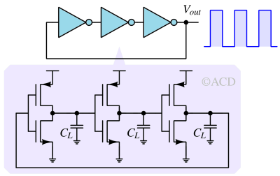
- Logical contradiction : The logical instability of an odd number of inverters forms the basis of a ring oscillator. As shown in the figure, the first NOT gate inverts the signal, so if the input of the first inverter is HIGH, its output becomes LOW. Consequently, the output of the last inverter in the series will also be LOW. When this output is fed back to the input of the first inverter, a logical contradiction arises, creating an inherently unstable circuit.
- Inverter delay : The second fundamental principle of a ring oscillator is the delay caused by each inverter. This delay is determined by the parasitic RC circuits at each stage. This delay means that after an input change, the inverter’s output will take some time to update, temporarily allowing the circuit to maintain the logical contradiction. The delay for each inverter corresponds to the time required for the capacitor to charge or discharge to reach the inverter's logical threshold.
Ring oscillator frequency formula
Each inverter is designed to be identical, ensuring identical time constants, thresholds, and amplitudes across all stages. As a result, the output frequency depends on the delay time Tdelay and the number of inverters N. Thus, the oscillation frequency can be adjusted by modifying either Tdelay or the number of inverters in the chain. The frequency (f) of ring oscillator can be expressed as :
$$f=\cfrac{1}{NT_{delay}}$$
Phase noise and jitter of ring oscillator
The supply, flicker, and thermal noise of transistors directly modulate the oscillation frequency, manifesting as phase noise/jitter. Phase noise is a frequency-domain view of the noise spectrum around the oscillator signal, while jitter is a time-domain measure of the timing accuracy of the oscillator period. Phase noise is expressed as dBc/Hz and measured relative to the center frequency (fo).
The phase noise is looks like :
$$S_{phi{}n}(f)=\alpha{}\left(\cfrac{f_o}{\Delta{}f}\right)^2$$
fo is the center frequency. Δf is the offset frequency from the center frequency fo.
Figure of merit of ring oscillator
The performance of the ring oscillators can be compared using the Figure of merit (FOM):
$$\text{FOM}=10\log{}_{10}\left(\cfrac{f_o^2}{\Delta{}f^2P_{mW}S_{\phi{}n(\Delta{}f)}}\right)$$
Ring oscillators have poor phase noise, which affects their FOM. Their FOM numbers are near 150, and those of LC oscillators are near 190.
KVCO or KVDD
This quantity often indicates the sensitivity of a voltage-controlled oscillator (VCO) to its control voltage (or supply voltage). The rate of change in frequency with a control voltage (Vctrl) is called KVCO. If this number is very high, the supply voltage noise can easily modulate the output voltage, causing random jitter and phase noise.
$$K_{VCO}=\cfrac{\Delta{}f}{\Delta{}V_{ctrl}}$$
Similarly, the rate of change in frequency with supply voltage (VDD) is called KVDD. It is expressed as the ratio of change in frequency with change in voltage.
$$K_{VDD}=\cfrac{\Delta{}f}{\Delta{}V_{DD}}$$
Temperature stability of ring oscillator
The frequency of a ring oscillator is determined by the delay (Tdelay) introduced by each inverter stage. This delay is heavily influenced by factors such as the inverter's rise and fall times, parasitic resistances and capacitances within the circuit, and the threshold voltages of the transistors. The rise and fall times are affected by transistor mobility and parasitic capacitances. The temperature coefficients of the dielectric material influence these parasitic capacitances. Parasitic resistances are contributed by metals and gate polysilicon, with metal resistance increasing with temperature and gate polysilicon resistance decreasing as temperature rises. These factors collectively make the frequency highly dependent on temperature, leading to poor temperature stability in ring oscillators.
However, by incorporating a feedback loop (PLL) with a temperature-insensitive reference, such as a quartz crystal, the frequency of the ring oscillator can be stabilized against temperature changes. This concept forms the basis for voltage-controlled oscillators, which will be discussed in the next section.
Single-ended ring oscillator and Differential ring oscillator
Ring oscillators are either single-ended or differential. The differences are mentioned below :
Single-ended oscillator
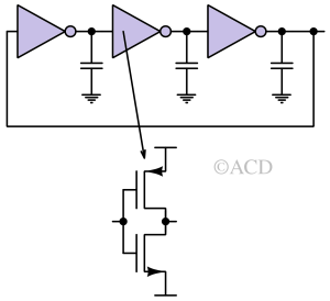
Each stage of this ring oscillator has only one input and one output. The most common is an inverter-based ring oscillator. Any noise at the supply comes directly at the output.
Differential ring oscillator
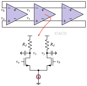
Each stage has two inputs and two outputs opposite each other (180° out of phase). This makes each stage reject common mode noise. The supply noise problem can be significantly alleviated using the differential ring oscillator because supply noise acts as a common-mode noise. In terms of noise (phase noise/jitter), differential ring oscillators are better than single-ended ring oscillators.
Ring oscillator VCO (voltage-controlled oscillator)
Ring oscillators can be configured to be used as voltage-controlled oscillators. These oscillators take significantly less area and are easy to design. Some of the ring oscillators with voltage control are mentioned below :
Inverters (NOT gates) based VCO
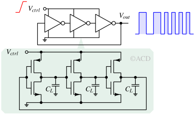
The inverter-based ring oscillator's supply voltage line is utilized as the control voltage. The supply voltage firmly controls the channel on-resistance. If the supply voltage increases, the channel resistance reduces dynamically, causing faster transitions and higher frequency. This topology's KVDD is very high, making it very sensitive to supply voltage noise. If using this inverter-based VCO, the LDO supplying the Vctrl line should make very low noise.
Differential ring oscillator-based VCO.
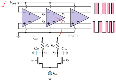
In a differential pair, as shown in the above figure, the charging and discharging currents are almost fixed. The discharging current is fixed to the ISS. While in the charging path, Rd does not reduce dynamically with an increase in Vctrl. This contrasts with inverters-based VCO, where the charging and discharging path’s resistances reduce strongly with an increase in Vctrl. This results in less dependency on Vctrl for frequency. The drain-bulk parasitic capacitance Cdb reduces with an increase in Vctrl. So, Cdb only controls the frequency as it is dependent on Vctrl.
Current starved Ring oscillator (CSRO)
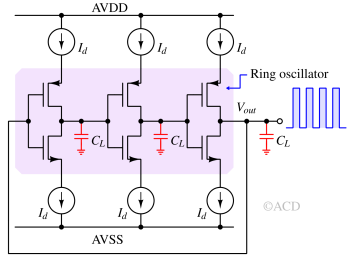
In a traditional ring oscillator, the source terminals of NMOS and PMOS are connected to the supply voltage (AVDD and AVSS). This allows any amount of current required to charge the parasitic capacitor Cp. The inverters act as voltage sources with some output resistances. This output resistance (Rp) and CL decide the Tdelay, which is very technology-dependent. The oscillation frequency cannot be accurately determined in simulation if modeling gaps exist.
The relationship between current and Tdelay is :
$$T_{delay}=\cfrac{V_{ampl}}{I_d/C_L}$$
The only technology-dependent parameter here is CL. Vampl is the amplitude of oscillation. A ring oscillator with only three stages does not allow the output to reach the supply rails due to significantly less loop delay. A higher number of stages enables the output voltage to reach the supply voltage due to a higher loop delay. In this case, with more stages, the Vampl could be written as (AVDD-AVSS), a known quantity.
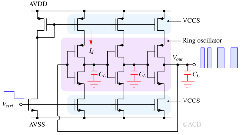
If the current is controlled by changing the voltage of the gate, the current source becomes a voltage-controlled current source. This way, we can also control the frequency (or Tdelay), creating the voltage-controlled oscillator (VCO).
Phases of a ring oscillator with an Odd number of stages
If there is an N single-ended stage, the ring oscillator can have N outputs. A single time-period has a phase shift of 2π.
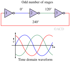
If there are an odd number of stages, then each output has a phase shift of :
$$\text{Phase shift}= (2k+1)\cfrac{2\pi{}}{N}=(2k+1)\cfrac{360}{N}^\circ{}$$ $$(k\in{}[0,N-1])$$
For example, in a three-stage single-ended ring oscillator, the phase shift associated with each stage is 120°, 240°, and 360°. Similarly, for a ring oscillator having six stages, the phase shift associated with each stage is 60°, 120°, 180°, 240°, 300°, and 360°.
Phases of a ring oscillator with an Even number of stages
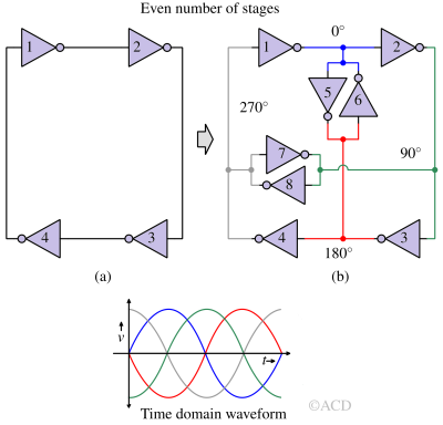
We saw earlier that an odd number of stages produces phases like 30°, 60°, 120°, etc. In applications like quadrature modulation, where In-phase (I) and Quadrature-phase (Q) signals are required, outputs having phase shifts of 45° or 90° are needed. This can be achieved using an even number of stages.
$$\text{Phase shift}= (2k)\cfrac{2\pi{}}{N}=(2k)\cfrac{360}{N}^\circ{}$$ $$(k\in{}[0,N-1])$$
Where N is the number of stages, there is one problem with the number of stages. The logical instability/contradiction is not there. It means that, given a state, Even-number of stages will hold that state indefinitely. To solve that, feedback is added using back-to-back inverters, as shown in Figure 10. This is done using inverters 5,6,7,8.
Ring oscillator process monitor
Ring oscillators (RO) are effective and practical Design-for-Manufacturability monitoring tools that capture performance variability caused by physical variations. They are compact, easy to design, and simple to implement. Commonly used as test structures in the scribe lines of selected wafers, ROs help silicon manufacturers monitor process variations and assess MOS device characteristics. By being strategically placed across the chip, ring oscillators evaluate the impact of these variations on standard cell delays and overall performance.
Advantages and disadvantages of ring oscillator
Some advantages and disadvantages of ring oscillators are mentioned below :
Advantages
- Ring oscillators have a much smaller footprint than resonant oscillators because they don’t require LC tanks or crystals. This makes them ideal for on-chip applications with strict area constraints.
- They are also straightforward to understand and design, with frequency easily adjusted by the number of inverter stages.
- Ring oscillators can be optimized for low power consumption.
- It has a wide tuning range.
- It has the smallest footprint among all oscillators.
- It provides multiple phase outputs.
Disadvantages
- Ring oscillators are known for having worse phase noise and jitter performance than resonant oscillators.
- Ring oscillators are also highly dependent on the chip's temperature, which is undesirable if exact frequencies are required.
Applications of the ring oscillator
- Process Monitoring : Used as test structures to monitor process variations and evaluate circuit performance in semiconductor manufacturing.
- Phase locked loops : It is a compact and easily tunable digital circuit and system clock source. It is used in applications requiring variable frequencies, and the number of inverter stages or delay elements can be adjusted to adjust the frequency.
- Low-Cost Signal Generation : Provides a simple and low-power solution for generating periodic signals in integrated systems.