Setup time
In a flip-flop setup time is the time duration before the clock edge when the incoming data needs to be settled. If the data changes after the setup time, metastability may occur.
Hold Time
The extra time required for the data to be held unchanged after the clock edge. Metastability may occur if data changes before hold duration.
Metastability in flip-flops
It is condition when the output of the flip-flop is uncertain due to setup or hold time violation (or maybe due to other reasons too). It assumes a state which is undesirable. Sometimes, it takes too long to settle to desired state.
Concept of setup time using example

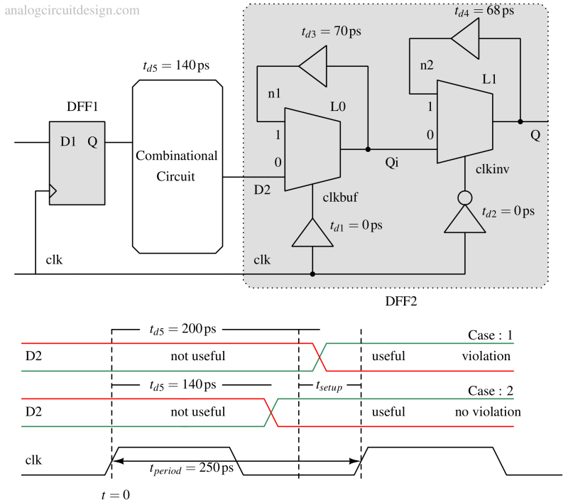
In Fig. 1, origin of setup time in flip-flop is explained. The clock feeds both DFF1 and DFF2. Both the DFF are rising edge triggered flip-flops. When the clock is 0, D2 and Qi are connected, however it takes (t_{d3} = 70,\text{ps}) for Qi to reach n1. It means that any change in D2 will appear at node n1 after (t_{d3} = 70,\text{ps}) delay, when clock is 0. After rising edge when clock is 1, n1 is connected to Qi and any change in D2 is ignored. It is very important to have both n1 and Qi settled to same value when clock is 0. It is because if they have different values due to delay and both n1 and Qi are connected together, there would be metastability. (t_{setup} = t_{d3} = 70,)ps.
Let's assume case (#1), where delay due to combinational logic is 200ps. D2 is changed after setup time window and clock is 0. Now, before value of D2 reaches n1 via Qi, rising edge arrives. It means, now n1 will be connected to Qi. n1 and Qi are different because value of Qi hasn't reached n1 due of delay (t_{d3}). Therefore metastability may arise. Therefore in case 1, setup violation is there.
In another case (#2), where clock rising edge arrives after n1 is settled (to same value as Qi). Now there would be no metastability. In Fig 1, the useful logic should reach D2 before 180ps (250ps - 70ps) so that the desired data has time to settle at node n1 and no setup violation occurs.
$$t_{period}-(t_{clk-Q}+t_{comb})>t_{setup}$$
(t_{clk-Q}) is the delay time it takes for data to appear at DFF1's Q after clk's rising edge. In this example it is considered 0 for simplicity. In this case, (t_{comb} = t_{d5}).
Some of the reasons for setup violations are :
1. High combinational logic delay. To deal with this, in design phase, the combinational logic which feeds the DFF is designed to have minimum delay such that the useful logic reaches before the (t_{period} - t_{setup}) from time (t=0) (i.e., previous rising edge).
2. Low time periods. If it is not possible to reduce the delay of the combinational logic then the time period is increased. By this way, rising edge is delayed and n1 is allowed to settle to D2 value. This solution is feasible even after chip is fabricated, however it impacts performance.
Concept of hold time using example

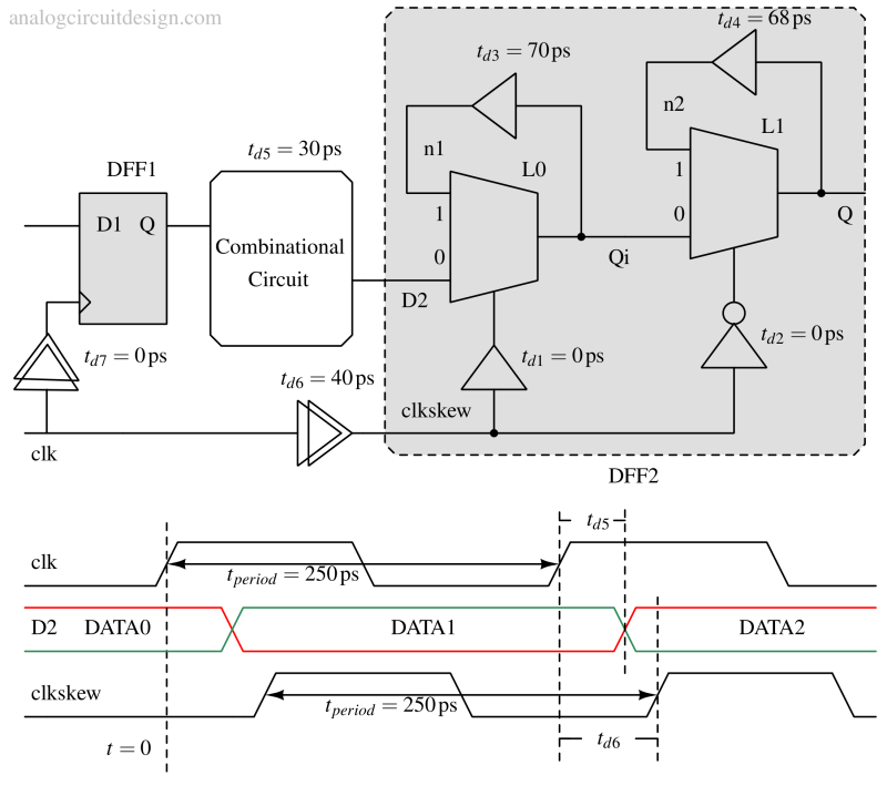
In Fig 1, the D2 value has the freedom to change immediately after the rising edge. This is because (t_{d1} = 0,)ps. So, hold time of this flip-flop is 0. However if a clock skew is there then there may be hold time violation. Now consider the scenario of Fig 2, where there is clock skew due to presence of (t_{d6}). Let's analyse the problem after time t = 250ps. Note that there are now two versions of clock, clk and clkskew. Clock skew means that there is shift in rising and falling edge due to delay. (t_{d6}) is an undesirable delay that occurs due to RC delay of clock routing or due to clock gating. D2's change from DATA1 to DATA2 is triggered by clk's rising edge. It is desired that DATA1 latches to DFF2 at clk's rising edge. The problem is, DFF2 is not latching to DATA1 at clk's rising edge. It is trying to latch to DATA2 because it is triggered by clkslew, however it will go to metastable state due to setup time violation. Therefore DFF2 is latched to unwanted data. It can be solved if (t_{d6}<t_{d5}) or by introducing equal skew ((t_{d7} = 40,)ps) in clk. It is must to correctly quantify the delays such that it can be rectified in design phase itself. Once chip is fabricated, there is no definite way to get rid of hold violation.
Suppose the clock's time period is increased to solve the problem. The delays will remain unchanged. If the delays remain unchanged then the problem is still there. So, changing the clock period does not solve the problem.
An inequality can be derived from the condition of hold :
$$t_{clk-Q}+t_{comb}-t_{skew}>t_{hold}$$
$$0+30-40not>0$$
By introducing (t_{d7}) to mitigate the hold violation, (t_{clk-Q} rightarrow{} t_{clk-Q} + t_{d7}). Substituting in the above equation,
$$t_{clk-Q}+t_{d7}+t_{comb}-{t_{skew}}>t_{hold}$$
$$0+t_{d7}+30\text{ps}-40\text{ps}>0\text{ps}$$
From above inequality it can be said that minimum value of (t_{d7}) should be 10ps. If this condition is fulfilled then DATA1 will be taken by DFF2 without any hold and setup violation.