Successive approximation (SAR) ADCs
Successive-approximation-register (SAR) analog-to-digital converters (ADCs) dominate the medium to high-resolution ADC market. SAR ADCs offer sampling rates of up to 25Msps and resolutions ranging from 8 to 18 bits. This architecture enables the creation of compact, low-power, high-performance ADCs.
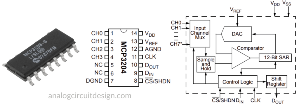
Internal components/architecture of SAR ADC
The successive-approximation analog-to-digital converter (SAR ADC) circuit is typically composed of four primary subcircuits:
- A Track-Sample-and-Hold circuit responsible for capturing the input voltage Vin.
- An analog voltage comparator that compares Vin with the output of the internal DAC and conveys the comparison result to the successive-approximation register (SAR).
- A successive approximation register subcircuit designed to provide an approximate digital representation of Vin to the internal DAC.
- An internal reference DAC that supplies the comparator with an analog voltage equal to the digital code produced by the SAR, which is used for comparison with Vref.

Working of a SAR ADC
A SAR ADC employs a straightforward architecture akin to a binary search. It starts with the analog input voltage (VIN) held in a track/hold circuit. Initially, an N-bit register is set to midscale (100... .00, with the most significant bit (MSB) as 1), which results in the DAC output being VREF/2. A comparison is made between VIN and the DAC output (VDAC). If VIN is greater than VDAC, the MSB remains 1; if VIN is less, it's set to 0. Then, the MSB-1 bit is set to 1 in the N-bit register, and the comparison process repeats. This sequence continues from the MSB down to the least significant bit (LSB) until the conversion is complete, providing the N-bit digital output within the register.
The internal circuitry may operate at a speed Nfs, where fs is the sampling rate and N is the number of bits.
Example of SAR ADC working
Following figure shows an example of a 3-bit conversion. The y-axis represents the DAC output voltage and corresponding register output. The sampled analog input is held till the conversion is complete. As in binary search, the input is predicted first by setting a bit to 1 and compared against the sampled analog input (Vin). If the sampled input is higher than predicted value (Vin > VDAC or VC = 1), the bit value = 1 is retained; otherwise (Vin < VDAC or VC = 0) the bit is set to 0.
Let’s denote the SAR register content as b2b1b0, the start po\int is MSB (b2) set to 1. It means DAC output is (1/2)VREF (because the SAR register is set to b2b1b0=1002). In the example, the first comparison shows that Vin < VDAC. Thus, b2 is set back to 0. The SAR register is then set to 0102 and the second comparison is performed. As Vin > VDAC, b1 remains at 1. Now b0 is set to 1, which means DAC is then set to 0112, and the third comparison is performed. Since Vin < VDAC, b0 is set back to 0 meaning DAC is set to 0102 and End of Conversion (EOC) flag is set to 1 signifying conversion is complete.

Challenges of designing a SAR ADC
The components which limit the linearity/precision/accuracy and speed of SAR ADC are:
- The settling time of the DAC, which must reach a level within the converter's resolution, typically around ½ LSB.
- The comparator's ability to resolve small difference between Vin and VDAC. Smaller the difference, smaller the gain and more time it takes to reach 1 or 0. The offset and noise affects the precision. Noise should be less than 1 LSB.
- Component mismatch and parasitics.
Advantages of SAR architecture over other types

As shown in the above figure, the SAR architecture provides a decent SNDR (dynamic range) at lowest energy per conversion. This make it suitable where power savings are important. Another advantage of SAR architecture (also for Flash ADC) that the conversion time is fixed without any dependency on the input value. This is unlike Delta-sigma where the conversion time is dependent on the input value at any instant.
Application of SAR ADCs
- Portable battery-powered instruments
- Pen digitizers
- Industrial control systems
- Data/signal acquisition systems.