Switch mode power supply (SMPS)
A Switch Mode Power Supply (SMPS) is a power supply that efficiently converts electrical power from one form to another using high-frequency switching. It is commonly used to provide regulated DC voltage for electronic devices.
SMPS vs linear regulators
Switch mode power supplies are much more efficient than linear voltage regulators. When there is a significant difference between input and output voltage, linear voltage regulators become inefficient.
The efficiency of switching regulators comes from the fact that there is no power loss due to any resistor. The switching regulator comprises switches and non-dissipative passive elements like inductors and capacitors. Energy is transferred from the inductor to the capacitor from one switching cycle to another. In a practical scenario, the switches have non-zero resistance, and the diodes have non-zero voltage drop, which causes energy loss. That is why, instead of being 100% efficient, switching regulators are 95-99% efficient. At low load currents, switching losses dominate, while at very high load currents, I2R losses dominate.
Regulator and converter
A regulator is a feedback system where the output is made equal to the reference voltage by continuously changing the duty cycle. A converter is just a fixed duty cycle system without feedback where the load behavior is well-known in advance. A converter is very simple in design while a regulator design is complex.
Switch mode power supply working principle
The main working principle of an SMPS involves the following steps:
Rectification (for AC-DC converters): The AC (alternating current) input from the power source is first rectified into DC (direct current). This is typically done using a bridge rectifier. Not all switching converters have AC-to-DC conversion features. Some are simply DC-DC converters that don't need rectification.
Filtering: The rectified DC voltage often has ripples. A filter, usually a capacitor, is used to smooth out these ripples and produce a more stable DC voltage.
Switching: The filtered DC voltage is then fed into a switching circuit. The heart of an SMPS is a semiconductor switch (often a transistor or a MOSFET) that rapidly turns on and off at a high frequency. This switching action is what gives the SMPS its name.
Transformer: The switched DC voltage is then fed into a transformer. The high-frequency switching allows the transformer to be relatively small in size compared to traditional transformers operating at lower frequencies.
Isolation: The transformer provides electrical isolation between the input and output, which is essential for safety and to prevent ground loops. Isolation is more common in AC-DC SMPS.
Output Regulation with Feedback Control: Most SMPS designs include a feedback control system. This system continuously monitors the output voltage and adjusts the duty cycle of the switching transistor to maintain a constant output voltage despite changes in input voltage or load conditions.
Pulse width modulation and duty cycle
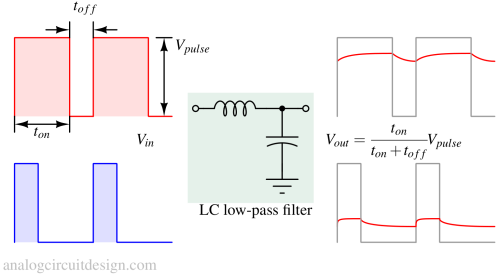
Pulse width modulation (PWM) is a standard technique to control the average voltage of a load. We call the ratio of turn-on time and time period of the signal the Duty cycle (D). This technique of modulating the duty cycle is helpful when we have only 2 voltage levels (Vpulse and 0).
$$D = \cfrac{t_{on}}{t_{on}+t_{off}}$$
Buck regulator
The Buck regulator takes a DC input voltage and produces a DC output voltage that is lower in magnitude than the DC input voltage (but having the same polarity).
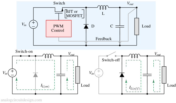
When the switch is ON: The difference between the input and output voltages across the inductor causes the current through the inductor to linearly increase. During the ON time, the inductor current flows into both the load and the output capacitor (the capacitor charges during this time).
When the switch is OFF : The input voltage applied to the inductor is removed. To maintain the same current before and after the switch is turned off, the voltage at the cathode of the diode will drop and become negative to turn on the diode. The inductor current then flows through the load and back through the diode.
$$V_{out}=\cfrac{t_{on}}{t_{on}+t_{off}}V_{in}=D\cdot{}V_{in}$$
Read more: Buck regulator
Boost regulator
The Boost regulator takes a DC input voltage and produces a DC output voltage that is higher in magnitude than the DC input voltage (but having the same polarity).
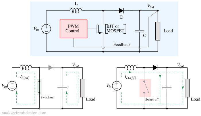
When the switch is ON : The input voltage is forced across the inductor which causes the current through it to linearly increase. The anode terminal of the diode is at zero potential and the cathode terminal is at a higher potential, so the diode is turned off. In this time, the load current is supplied entirely by the capacitor.
When the switch is OFF : The anode of the diode becomes positive to maintain the inductor current after the switched is turned off. The inductor current flows through the forward biased diode to supply current to the load and simultaneously charge the capacitor.
$$V_{out}=\cfrac{1}{1-\cfrac{t_{on}}{t_{on}+t_{off}}}V_{in}=\cfrac{1}{1-D}V_{in}$$
Read more: Boost regulator
Buck-boost regulator (Inverter)
The Buck-Boost (Inverting) regulator takes a positive DC input voltage and produces a negative DC output voltage that is opposite in polarity to the input. The negative output voltage can be either larger or smaller in magnitude than the input voltage.
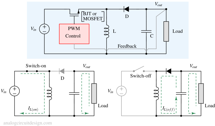
When the switch is ON: The input voltage is forced across the inductor, which causes the current to increase linearly with time. The cathode (Vin) of the diode is at a higher potential than the anode (Vout). So, the diode is turned off. During this time, the load current is supplied entirely by the capacitor.
When the switch is OFF: The current through the inductor causes the cathode to become negative. The cathode voltage will drop till the diode becomes forward-biased to allow the current to flow. This current charges the capacitor and also provides current to the load.
Read more: Buck-boost converter.
Flyback regulator
The flyback converter uses a coupled inductor (or a transformer), to isolate the converter’s input from its output. The input is connected to the transformer's primary windings and the output is connected to the secondary windings. The flyback topology is very popular in AC-DC conversion like portable device chargers, LED power supplies, etc.
Flyback converters operate in either continuous mode (where the secondary current is always > 0) or discontinuous mode (where the secondary current falls to zero on each cycle).
A flyback topology can provide multiple outputs. In this case, one of the outputs (usually the highest current) is used to provide the PWM feedback to the control loop. Other secondary windings are regulated through LDOs.
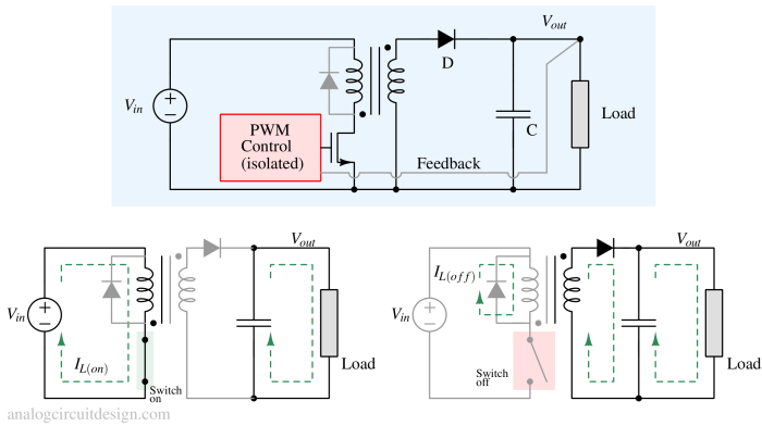
When the switch is ON : The input voltage is forced across the transformer's primary coil which causes the current through the primary coil to increase linearly. Because of the dot placed in opposite direction, a negative voltage is induced in the secondary coil. This reverse biases the diode. During this time, the load current is supplied by the output capacitor alone.
When the switch is OFF: The dot side in the primary side becomes more positive which induces positive voltage at the dot side of the secondary windings. This forward biases the diode and let the secondary current flow to the capacitor and the load.