Switched Capacitor Filters
Switched capacitor filters offer several advantages, including the ability to implement high-pass filtering with a relatively small number of passive components and without the use of inductors. They can be easily integrated into integrated circuits, making them popular in modern analog and mixed-signal designs.
Better process variation control because the resistor in a filter is also implemented using capacitors. So, the cutoff/center/notch frequency is well controlled because the process-corners variation is due to the capacitor only.
Principle of switched capacitor filters
The idea is to use a capacitor to transfer the exact amount of charge from one terminal to another as a resistor in time (1/F).
Switched capacitor resistor
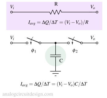
The above figure shows the equivalent switched capacitor implementation in the discrete-time domain for a resistor in the continuous-time domain. Equating the average current of the continuous time resistor and the switched-capacitor resistor, we get
$$\cfrac{V_i-V_o}{R}=\cfrac{(V_i-V_o)C}{\Delta{}T}$$
$$\implies{}R=\cfrac{\Delta{}T}{C}=\cfrac{1}{C.F}$$
Switched capacitor low pass filter
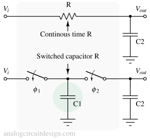
Switched capacitor's low pass filter's cutoff frequency :
$$f_{-3dB}=\cfrac{1}{2\pi{}}F\cfrac{C_1}{C_2}$$
The above expression depends only on mismatch because C1 and C2 are made of the same material. The mismatch is usually <0.1% for integrated circuit implementation. Also, the 'F' is accurate to the order of 'ppm'. So, the f-3dB is very well controlled. Variation is less than <0.1%.
Continuous time resistor low pass filter's cutoff frequency :
$$f_{-3dB}=\cfrac{1}{2\pi{}}\cfrac{1}{RC_2}$$
Here, f-3dB depends on the process variation because R and C are made of different materials. Usually, process variation is 20% for each component. So, f-3dB can vary by 40% in the worst case.
Switched capacitor integrators
Instead of using traditional resistors and capacitors for integration, switched capacitor integrators use a series of switches and capacitors. These switches control the charging and discharging of the capacitors in a manner that simulates the effect of an integrator.

As shown in Fig 3, An integrator can be made using a switched capacitor resistor. We can understand the circuit conceptually. In phase 1 (φ1), the capacitor Cs (also called sampling capacitor) is charged to Vin. This charge is transferred completely to Ci (also called integrating capacitor) in phase 2 (φ2). The top plate of the capacitor is connected to the virtual ground node and the bottom plate is connected to the ground in this phase, so the charge remaining in Cs is zero. The Ci acts as a charge reservoir where every charge sampled by Cs is accumulated resulting in a step-wise voltage increase at Vout. If Vin is negative in some cycle, the charge is taken out from the Ci, and Vout drops from the previous voltage.
Switched capacitor integrator's sensitivity to parasitic capacitor
Parasitic capacitors can introduce errors in the integrator due to extra charge injection. As shown in Fig 3, there are mainly three parasitic capacitors that may affect our output signal Cp1, Cp2, and Cp3. Cp1 is the top plate is connected to the output of the opamp, so not a problem. Opamp will supply the extra charge to Cp1 from supply. Cp2's top plate always sees the virtual ground while the bottom plate is connected to the ground. So, it does not store any charge. This is also not a problem.
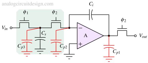
A parallel capacitor (Cp3) to the ground connected at the top plate of Cs can inject extra charge from Cs to Ci. This introduces errors in the output of the opamp.
Parasitic insensitive switched capacitor integrator
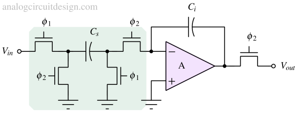
In Figure 5, a parasitic insensitive switched capacitor integrator is shown. It utilizes a Cs (called here flying capacitor) and instead of two switches in the previous implementation (Fig 3), it uses four switches. The integrating action is similar to the previous implementation.
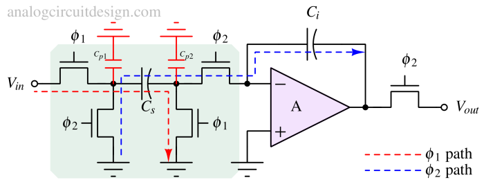
In phase 1, Cp1 is charged to Vin. However, in phase 2, Cp1 is discharged through the ground due to a switch to the ground. The charge does not enter Ci.
In phase 1, Cp2 is grounded while in phase 2, Cp2 is connected to virtual ground. Therefore no charge is present in Cp2 during both phases.
Switched capacitor noise
The switches and the opamp are the sources of noise in the switched capacitor networks. The finite resistance of the switches introduces thermal noise. Opamp itself introduces flicker and thermal noise due to internal transistors.
Switched capacitor integrator noise
The overall integrated noise of the switched capacitor integrator is :
$$v_n^2=\cfrac{kT}{C_s}$$