Transmission gates
A transmission gate, also known as an analog switch, is an electronic component designed to control the passage of signal levels from the input to the output. This solid-state switch comprises a PMOS transistor and an NMOS transistor to support both logic states (High and Low). By biasing the control gates complementarily, both transistors can either be turned on or off simultaneously. Usually, the transmission gates are bidirectional. This means the signal can flow from input to output and vice-versa.
Transmission gate symbol and schematic
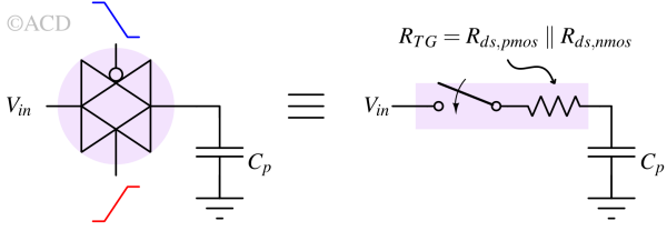
To make a transmission gate, two MOS transistors (one PMOS and one NMOS) are arranged in parallel. There is an inverter placed between the gate terminals of the NMOS and PMOS transistors to provide complementary control voltages. This is because NMOS turns on when the gate is high while PMOS turns on when the gate is low. When the CONTROL signal is low (zero), both the NMOS and PMOS transistors are in a cutoff state, resulting in an open switch. Conversely, when CONTROL is high (one), both transistors are biased to conduct, effectively closing the switch.

Therefore, the transmission gate functions as a "closed" switch when CONTROL = 1 and operates as an "open" switch when CONTROL = 0, serving as a voltage-controlled switch. The symbol representing the gate of the PMOS FET is indicated by a bubble.
Transmission gate working principle
To grasp the functionality of a transmission gate, it's essential to comprehend the operations of NMOS-only and PMOS-only switches/transmission gates separately. We will try to understand the behavior when the transistors are turned on. When transistors are turned off, the output becomes a High-Z node. High-Z means the input resistance of the node is very high (open circuit).
NMOS-only switch or transmission gate

In the NMOS switch, the gate is tied to VDD, and the body is tied to VSS to turn on the transistor. If a rising pulse is given at the input, we can see that the output is rising slowly to VDD - Vtn. Vtn is the threshold of the NMOS transistor. Ideally, it should rise fast and rise up to VDD. The waveform is rising slowly because the VGS of the NMOS is decreasing, which is increasing the channel resistance (Rds,on). This reduces the current to charge any parasitic capacitor (Cp) at the output. The current reduces to zero and Rds,on becomes infinite when the output reaches VDD-Vtn. This does not let output go above VDD-Vtn.

If a falling pulse is given at the input, we can see that the output is falling fast to VSS. The waveform is falling fast because the VGS of the NMOS is increasing, which is decreasing the channel resistance (Rds,on) rapidly. This increases the current to discharge any parasitic capacitor (Cp) at the output. The current discharge the parasitic capacitor to the input voltage level (VSS).
So, we can observe that the NMOS behaves very well when there is a falling waveform at the input.
PMOS-only switch or transmission gate

In the PMOS switch, the gate is tied to VSS, and the body is tied to VDD to turn on the transistor. If a falling pulse is given at the input, we can see that the output is falling slowly to Vtp. Vtp is the threshold of the PMOS transistor. Ideally, it should fall fast and fall up to VSS. The waveform is falling slowly because the VSG of the NMOS is decreasing, which is increasing the channel resistance (Rds,on). This reduces the current to charge any parasitic capacitor (Cp) at the output. The current reduces to zero and Rds,on becomes infinite when the output reaches Vtp. This does not let output go below Vtp.

If a rising pulse is given at the input, we can see that the output is rising fast to VDD. The waveform is rising fast because the VSG of the NMOS is increasing, which is decreasing the channel resistance (Rds,on) rapidly. This increases the current to charge any parasitic capacitor (Cp) at the output. The current charges the parasitic capacitor to the input voltage level (VDD).
So, we can observe that the PMOS behaves very well when there is a rising waveform at the input.
NMOS and PMOS in parallel

When a rising input is given at the input of the transmission gate, NMOS's output ceases to move beyond VDD-Vtn however PMOS supplies the necessary current to the parasitic capacitor to charge to VDD.

When a falling input is given at the input of the transmission gate, PMOS's output ceases to move below Vtp however NMOS supplies the necessary current for the parasitic capacitor to discharge to VSS.
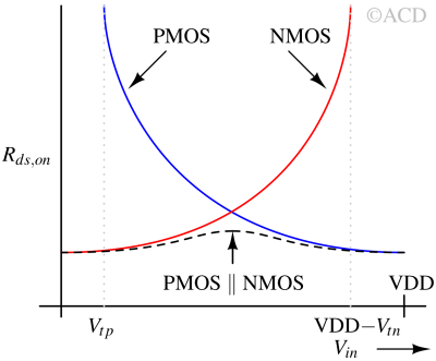
 The overall equivalent resistance (RTG=Rds,pmos||Rds,nmos) of the transmission gate (TG) remains consistently stable, exhibiting almost no dependency on the output voltage. In contrast, the separate equivalent resistances of the NMOS and PMOS transistors show significant reliance on Vin or Vout. This attribute of the CMOS transmission gate is inherently advantageous and desirable.
Transmission gate model for circuit analysis

A transmission gate can be modeled as a closed switch offering a minimum resistance RTG. When the transmission gate is opened, the switch can be assumed to be open. This model is used extensively in the modeling of Sample and Hold circuits in ADCs. RTG is actually a nonlinear resistor which is a major source of distortion is ADC. To solve it, Bootstrapped transmission gates are used to keep the RTG even more constant.
Transmission gate truth table and tristate buffer

Table 1 : Truth table of transmission gate
| Control | A | B |
|---|---|---|
| 0 | 0 | High-Z |
| 0 | 1 | High-Z |
| 1 | 0 | 0 |
| 1 | 1 | 1 |
The transmission gate opens the connection between A and B when Control is zero. That is why the output goes to High-Z mode, where the resistance of node B is very high. When control is high, the signal at A is allowed to move to B. Please note that the truth table of the transmission gate now consists of three states namely 0, 1, and High-Z. That is why a transmission gate is also called a Tristate buffer.
Transmission gate verilog code
module gate_modeling(input A,ctrl,output B_bufif1,output B_bufif0);
//transmission-gate with control signal
bufif1(B_bufif1, A, ctrl);
//transmission-gate with inverted control signal
bufif0(B_bufif0, A, ctrl);
endmodule
Transmission gate multiplexer (MUX)

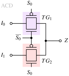
When the control signal S0 is in a low state, the upper transmission gate activates, allowing the passage of I0 through it. Simultaneously, the lower transmission gate deactivates disabling the passage of I1 through it. Consequently, the output becomes equal to I0.
Similarly, when the control signal S0 is in a high state, the upper transmission gate de-activates, cutting off the passage of I0 through it. Simultaneously, the lower transmission gate activates enabling the passage of I1 through it. Consequently, the output becomes equal to I1.
This transmission gate (in Fig 10) can transmit analog signals also.

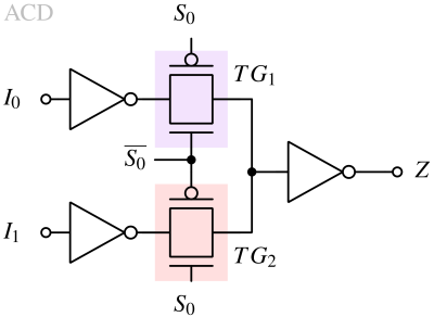
To isolate the input from successive logic and increase the fan-out of the transmission gate, inverters can be added as shown in the above figure. Due to the addition of inverters, this transmission gate no longer supports analog signals. Now, it can only support digital signals.
Transmission gate applications
- Transmission gates serve as fundamental components in constructing logic circuits, including elements like a D Latch or D Flip-Flop.
- Transmission gates are used to sample and hold circuits in ADCs. The switch is closed when the sample capacitor is required to be charged to the input voltage. The switch is opened when the capacitor needs to hold the charge while the input is varying.
- Also, a transmission gate has the capability to isolate components from active signals during processes like hot insertion or removal.
- In security applications, these gates can be utilized to selectively prevent the transmission of crucial signals or data unless there is proper hardware-controlled authorization, adding an additional layer of security and control to the system.