Voltage differentiator
A voltage differentiator is an electronic circuit that differentiates an input voltage signal with respect to time and shows the result at the output. In mathematical terms, it calculates the rate of change of the input voltage signal, also known as the derivative of the voltage signal.
The circuit for an Op Amp-based voltage differentiator typically consists of an operational amplifier, resistors, and capacitors. The basic configuration of voltage differentiator using op amp is shown below:

Opamp differentiator characteristics
The transfer function of this circuit is given by:
$$V_o=-sR_FC_iV_i$$
Where Vo(s) is the Laplace transform of the output voltage. Vi(s) is the Laplace transform of the input voltage and s is the Laplace domain variable.
Voltage differentiator working principle
The current through the capacitor is proportional to the rate of change of the input voltage with respect to time C.(dV/dt). That current flows through the feedback resistor RF. This means that the output voltage (Vo) is a scaled version of the derivative of the input voltage (Vi). 
To derive the transfer function of the Op Amp-based differentiator, we can apply KCL at node vx,
$$\cfrac{v_i-v_x}{1/sC_i}+\cfrac{v_o-v_x}{R_F}=0$$
$$v_o=-Av_x$$
$$\implies{}v_x=-\cfrac{v_o}{A}$$
In an ideal opamp, the gain (A) is infinite, so node vx will be equal to zero. So,
$$\cfrac{v_o}{v_i}=-sC_iR_F$$
DC
When a DC voltage is applied to the input of a voltage differentiator, the output does not change. This is because the input capacitor blocks DC. So, there is no current through RF. Hence the voltage at vx = 0 and consequently voltage at output is 0.
AC

The AC response of a differentiator circuit looks like Figure 3. With frequency, the gain increases at 20dB/dec. The feedback resistance (RF) remains constant while the impedance of the input capacitance decreases with frequency. This means that the current through the capacitance increases with frequency. This increased current flow through RF produces a higher voltage at the output. Comparing it with inverting gain op amp, we can express the gain as the ratio of RF and 1/jωCi. It can expressed as below :
$$\cfrac{V_{out}}{V_{in}}=-\cfrac{R_F}{1/j\omega{}C_i}=-j\omega{}R_FC_i$$
The phase plot shows that there is a phase advancement of 90°. This means that the output waveform will be ahead of the input sine wave for a sine wave by 90°. If the input is \sin(ωt), the output would be cos(ωt).
Transient
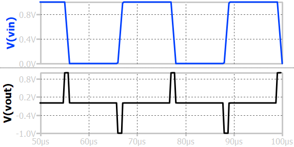
If a square wave is provided as an input, the voltage differentiator reacts during the edge transition. This is because, during edge transition, a current C(dV/dt) flows through the input capacitor.
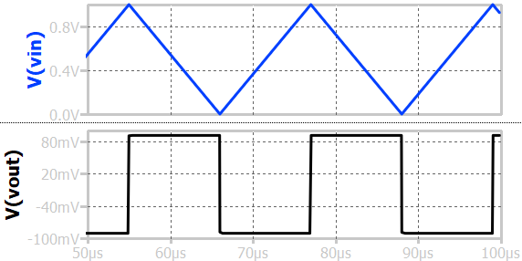
For a triangular wave input, the differentiator circuit will produce an output proportional to the slope of the triangular wave. When the input moves up, the current goes into the capacitor, and the output is negative voltage. The magnitude is constant because the rate of change (dV/dt) is constant. Similarly, when the input goes down, the magnitude is constant (proportional to the rate of change) and positive.
Finite high frequency gain differentiator
The circuit shown in Figures 1 and 2 has some limitations. The Op Amp can become unstable due to large RF and a moderate parasitic capacitor Cp. This forms a non-dominant pole near the amplifier's unity-gain bandwidth, degrading the phase margin. Reduction in phase margin can cause excessive ringing at the output or even sustained oscillation. So, a zero is introduced using CF (Fig. 5) to eliminate this pole. This CF and RF introduces a zero at 1/RFCF frequency and restores the phase margin.

Adding CF starts reducing the gain at high frequency. Beyond frequency 1/RFCF, the impedance offered by CF reduces. Ci acts as a short circuit. The combination of Ri, Ci, RF, and CF forms a bandpass filter. The circuit can be used as a differentiator below the upper cutoff frequency of 1/RFCF. The mid-band gain is set by Ri and RF, which can be represented as follows:
$$G=-\cfrac{R_F}{R_i}$$
It's important to note that this circuit is sensitive to high-frequency noise and may require filtering to remove unwanted noise and stabilize its operation.

Application of voltage differentiator
Some applications of voltage differentiator are listed below:
Edge detector circuit
Edge appears at the part of the signal where there is a change. A voltage differentiator can be used to detect such changes. Any change will force a current through the capacitor, which flows through Rf and produces output. This output can be compared against a threshold to detect a change.