Zener Diode
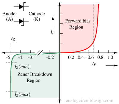
A Zener diode behaves as an ordinary PN junction diode in forward bias. However, unlike a conventional diode which blocks the current flow in reverse bias up to a large reverse breakdown voltage (typically 25V, 50V), the Zener diode is designed to conduct a lot of current at a relatively low reverse breakdown voltage called Zener breakdown voltage, VZ (typically 3.3V, 5.1V etc.)
Zener diodes are intentionally doped higher than regular PN junction diodes, so the reverse breakdown is more like Zener breakdown, not Avalanche Breakdown. A higher doping level makes the depletion region thin which causes a higher electric field in Zener diodes than in regular PN junction diodes.
Zener breakdown
When a reverse bias is applied across a heavily doped junction (as in the Zener diode), the valence band in the P-side region rises above the conduction band in the N-side region of the diode. Since the depletion region width in the Zener diode is lesser than the regular PN junction diode, the electric field is an order of magnitude higher.
This higher electric field enables the tunneling of electrons from the valence band (of the P-side) to the conduction band (of the N-side). This leads to a sudden high electric current in reverse bias.
Zener breakdown is reversible if the current is limited to avoid thermal damage (burnout).
Difference between Zener and Avalanche breakdown
Zener breakdown happens because of the tunneling of electrons while Avalanche breakdown happens due to multiplication. In avalanche breakdown, the high electric field causes electrons to get enough energy to knock out other electrons.
Both Zener and Avalanche breakdowns are reversible if the current is limited to avoid a rise in junction temperature above the device's limits.
Zener diode current-voltage characteristics

Zener diodes are intentionally used in reverse bias mode. This is because, for large variations of current from IZ(min) to IZ(max), it can regulate the voltage at VZ.
If the current falls below IZ(min), the voltage drops below VZ. If the current goes beyond IZ(max), then the Zener diode can be destroyed due to heating.
In the Zener breakdown region, the Zener diode act as a voltage regulator. This behavior protects other delicate electronic components in case of any voltage surge.
Zener diode as a voltage regulator and reference

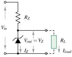
Zener diodes are commonly used to protect delicate circuit components from overvoltage. For this, the Zener diode is reverse-biased at IZ(max). If the load current is too high, then it can starve the Zener diode to the unregulated region when the current through it is less than IZ(min).
$$R_Z = \cfrac{V_{in}-V_Z}{I_{Z(max)}}$$
$$I_{Z(max)}=\cfrac{P_{max}}{V_Z}$$
$$I_{load}<I_{Z(max)}-I_{Z(min)}$$
VZ has to be reasonably high voltage in comparison to VF because it allows other circuits (connected to Vout) to be functional. VF is the forward voltage drop of regular P-N junction.
Example 1
The circuit shown in the above figure is used to provide regulated voltage (VZ=5.1V) across the RL=500. What is the value of RZ and the minimum required power dissipation rating of the diode? (Assume that the Zener diode has a constant reverse breakdown voltage for a current range, starting from IZ(min)=1mA to its IZ(max). The input voltage Vin can vary 10% from its nominal value of 7V. The resistance of the diode in the breakdown region is negligible.)
$$I_{load}=\cfrac{5.1}{500}=10.2\text{mA}$$
$$6.3\text{V}\leq{}V_{in}\leq{}7.7\text{V}$$
Minimum current will flow when Vin=6.3V and maximum current flow when Vin=7.7V for a fixed RZ. The maximum current should be within the power ratings of the Zener diode, while the minimum current should always be more than IZ(min) for proper voltage regulation.
$$R_Z=\cfrac{6.3\text{V}-5\text{V}}{1\text{mA}+10.2\text{mA}}=116\Omega{}$$
Current through Zener diode (IZ) when Vin=7.7V,
$$I_Z=\cfrac{7.7\text{V}-5.1\text{V}}{R_Z}-I_{load}=12.21\text{mA}$$
So, the required power rating is,
$$P_{Z}=5.1\text{V}\times{}12.2\text{mA}=62.2\text{mW}$$
From a design point of view, the above power rating is a minimum requirement. However, consider a situation where the load suddenly turns off, then the entire (7.7-5.1)/RZ current has to flow from the Zener diode. So, a safer power rating should come from the situation when Iload=0. In this situation, IZ :
$$I_Z=\cfrac{7.7\text{V}-5.1\text{V}}{R_Z}=22.4\text{mA}$$
$$P_{Z}=5.1\text{V}\times{}22.4\text{mA}=114.2\text{mW}$$
Zener diode series and back-to-back connections

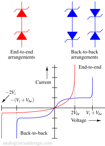
Using a back-to-back arrangement of Zener diodes in series, one can create a current limiter that provides a clipped AC wave. For End-to-end arrangements, its current-voltage curve will look like the typical current-voltage curve for a single Zener diode.