Small Signal Model
Real transistors are nonlinear elements. So it can become prohibitively complex to analyze even simple circuits. Therefore, it is converted to a linear system using Taylor series expansion near a bias point. In practice, the small-signal analysis holds true for almost every analog circuit.
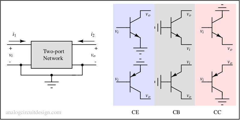
Usually we use 2-port model to represent a transistor. We keep one terminal from each port as reference node (gnd).
$$I_B(V_{BE}+\Delta{}V_{BE}) = I_B(V_{BE})+\underbrace{\left(\cfrac{\Delta{}I_B}{\Delta{}V_{BE}}\right)}_{1/r_{\pi{}}}\Delta{}V_{BE}$$
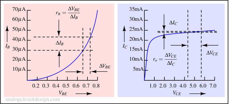
Low frequency model
In low frequency there is no effect of circuit capacitance. Input small-signal resistance is derived from \(I_B\) vs. \(V_{BE}\) curve. Output small-signal resistance is obtained from \(I_C\) vs. \(V_{CE}\) curve (Early effect). \(\beta{}\) is obtained from Gummel plot.
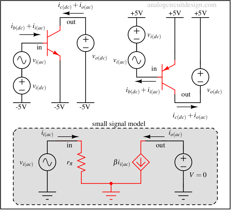
In following figure, the small signal model is shown as CCCS and VCCS. Both are correct. If \(\Delta{}I_B\) is known, it is convenient to use CCCS. If \(\Delta{}V_{BE}\) is known, it is more convenient to use VCCS.

$$r_{\pi} = \cfrac{V_t}{I_B}$$
$$V_t = \cfrac{kT}{q}$$
$$r_o = \cfrac{V_A}{I_C}$$
$$g_m = \cfrac{I_C}{V_t}$$
High frequency model
In high-frequency operation, we can add the capacitance related to various ports into the BJT model. This model can be used at low frequency also where we can assume capacitors to be open circuits.
The transconductor shown in following figure can also be represented as CCCS depending on the fact that whether input current is known or input voltage is known. The relationship to convert the VCCS to CCCS is :
$$g_mv_{be} = \beta{}i_b$$
$$g_m = \cfrac{\beta{}}{r_{\pi}}$$
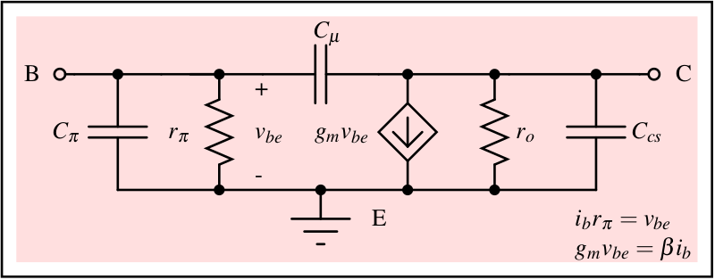
$$C_{\pi} = C_b + C_{jbe}$$
The input capacitor \(C_{\pi}\) is formed by 2 capacitors in the BJT :
- \(C_b\) : It is the base charging capacitance. \(C_b = \tau{}_Fg_m\).
- \(C_{jbe}\) : It is the forward bias junction capacitor. \(C_{jbe} = C_{jbe0}/\sqrt{1-V_{BE}/\psi{}_0}\) for \(V_{BE}\leq{} \psi{}_0/2\)
Amplifier configurations (2-port models)
There are 3 small signal two-port models used for BJT known as:
- Common Emitter (CE)
- Common Base (CB)
- Common Collector (CC)
These 3 configurations form the building blocks of amplifiers and many other analog electronics systems. Various permutations of these help in building very large analog systems.
Common emitter (CE)
In this configuration, the emitter is tied to a DC voltage. No signal is provided at the emitter. The input voltage signal is provided to the base. Output is captured as a current at the collector terminal because output (collector terminal) acts as a current source. To measure the current at the collector, the collector is held at a constant voltage \(V_{o(dc)}\). If the output current is flown through a large resistance, a large voltage gain can be obtained. In the case of BJTs, the input resistance of the CE amplifier is \(r_{\pi}\). So, it is low in comparison to the FET-based CS amplifiers. Output impedance is usually very high \(r_o = V_A/I_C\), a similar order for FET-based CS amplifiers.
This configuration can be termed a voltage-controlled current source (VCCS) because the input is a voltage and the output is a current.
Common base (CB)
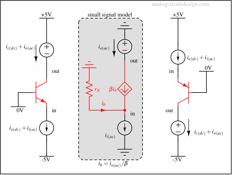
In this configuration, the base terminal is tied to a DC voltage. No signal is given to the base terminal. The input signal is provided at the emitter terminal in form of current because input impedance is low (~lower than FET-based amplifier as well for same current). Output is captured as a current at the collector terminal because output impedance is very high.
This configuration behaves like a current-controlled current source (CCCS) because the input is a current and output is also a current.
Why input should be current in CCCS?
It is because the input impedance is very low. If a voltage is formed at the input, it will require a large current to enforce that voltage at the input. Or if it is okay to take a hit in voltage level, then there exists a CC-CB compound stage which has a lot of advantages. More about the CC-CB compound stage in this article.
Common collector (CC)
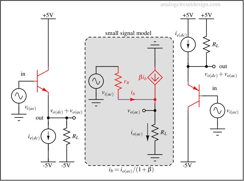
In this configuration, the collector terminal is tied to a DC voltage. No signal is given to the collector terminal. The input signal is provided at the base terminal in form of voltage because input impedance is fairly high (but lower than a FET-based amplifier). Output is captured as the voltage at the emitter terminal because output impedance is very low (so, emitter is acting as a voltage source).
This configuration behaves like a voltage-controlled voltage source (VCVS) because the input is a voltage and the output is also a voltage. The voltage gain is usually \(\leq{} 1\).
What do we mean by “output is also a voltage”?
We mean that the output terminals maintain the desired voltage across a load without the voltage level getting too much attenuated. Output voltage is not attenuated only if the output resistance of the source is much lower than the load resistance.
Small signal resistances
Base spreading resistance (also called 'rb')
This resistance represents the bulk resistance seen from the metal contact to the actual base region. It is responsible for the thermal noise in BJT. It is in the order of few ohms.
Base emitter resistance (also called 'r-pi')
It is the small-signal resistance derived from input characteristics of the BJT (Gummel plot). Since it is not a physical resistor in the BJT, it does not contribute any noise.
Output resistance (also called 'r-o')
Usually BJT and MOS behave like current source if input is tied to constant DC voltage. Output current of ideal current source should remain constant with the voltage applied. However, this does not happen in BJT/MOS.
In BJT, the output current rises with increases in collector-emitter voltage. This is because the base-collector depletion region widens. This shrinks the area where recombination of electrons-holes in base region can happen.
Since the current \(I_E\) generated from the emitter side is only dependent on VBE, \(I_E\) is independent of VCE. The shrinkage in base region reduces the base current because now it is lesser chance for recombination. That reduced base current flows though the collector. So, the collector current is increased. Basically it can be assumed that \(\beta{}\) is increased.
$$I_C = I_Se^{\left(\cfrac{V_{BE}}{V_t}\right)}\left(1+\cfrac{V_{CE}}{V_A}\right)$$
\(V_A\) is the early voltage.
Capacitances
Base charging capacitance
When there is a change in VBE, the charge density profile of the base region changes. The change in voltage and the corresponding change in charge defines the base charging capacitance \(C_b\).
$$C_b = \tau{}_Fg_m$$
\(\tau{}_F\) represents the base transit time of the charge carriers. Intuitively, it is the time spent by an electron in NPN transistor to cross the base region.
\(g_m\) is the transconductance of the BJT when biased in forward-active region.
Base-Emitter and Base-Collector depletion capacitance
In a p-n junction diode we learnt that in zero-bias state a depletion region is formed. This depletion region widens if we put a reverse-bias. In forward bias the depletion region shrinks but does not vanishes and it is still present in base-emitter junction. If the width of the depletion region shrinks, the capacitance increases. This depletion region in forward bias at base-emitter junction forms the base-emitter depletion capacitance.
$$C_{jbe} = \cfrac{C_{jbe0}}{\sqrt{1-\cfrac{V_{BE}}{\psi{}_0}}} \ \text{for} \ V_{BE} \leq{} \psi{}_0/2$$
The base-collector depletion region widens with higher VCE. With widening of the base-collector depletion region, the capacitance reduces. This capacitance is represented by base-collector depletion capacitance.
Base-Emitter and Base-Collector overlap capacitance
Lorem ipsum dolor sit amet, consectetur adipiscing elit. Ut elit tellus, luctus nec ullamcorper mattis, pulvinar dapibus leo.
Noise sources
Thermal noise (or Johnson-Nyquist noise)
Any physical resistor would cause thermal resistance. It is due to random motion of electrons due to freely available thermal energy. It is always present even if the external current or voltage across is zero.
\(r_b\) is responsible for thermal noise in BJT. For \(r_b\), thermal noise spectral density is :
$$\overline{v}^2 = 4kTr_b$$
As seen in the above formula, thermal noise is directly proportional to temperature \(T\).
The time domain distribution of amplitude is Gaussian.
Shot noise
This noise is associated with the charge carriers crossing the junction in random manner. In a forward biased junction, carriers move randomly but have a mean velocity in the intended direction. The flow of carriers are not streamlined flow.
Shot noise is prominent in devices where main current flows through a junction. It is not dependent on temperature. It is proportional to the current magnitude. The noise spectral density is :
$$\overline{i}^2 = 2qI_D$$
The above equation is valid till \(\Delta{}f\leq{}1/\tau{}\), where \(\tau{}\) is the depletion region transit time of the electrons.
The time domain distribution of peak-amplitude is Gaussian.
Flicker noise (or 1/f noise)
It is mainly caused by trapped charge capture and release in random fashion. In BJT, the flicker noise is much less than MOSFET.
It is represented as a current source in shunt with the trans-conductance model of BJT.
$$\overline{i}^2 = \cfrac{2qf_LI_B^{\gamma{}}}{f}$$
The time domain distribution of peak-amplitude is Gaussian.
Popcorn noise (Burst noise)
It represents the random step change in average value of noise in time domain. Either a sudden increase in noise level of base current in BJTs or change in threshold of MOSFETs. The popcorn noise appears for frequency less than 1kHz.
It got the name of popcorn noise because, if the device is amplified to audible sound, it resembles cooking popcorns.
The time domain distribution of peak-amplitude is non-gaussian.
