Introduction
A BJT is a 3 terminal semiconductor-based transistor. All the terminals of the BJT are connected to the body through a metal-semiconductor junction. Unlike FET, there is no channel formation/depletion through controlling voltages in BJTs. It is called bipolar because charges having both polarities (electrons and holes) are involved in conduction. The word junction comes in BJT because a forward-biased p-n junction decides the electrical behaviour of the device.
Major advantages of BJT over MOSFET are :
- High current driving capability (because the current is dependent on barrier dependent thermal diffusion not drift)
- Reliability (due to absence of thin oxide insulation)
- High frequency of operation (due to higher transconductance in the same area as of MOSFET).
BJTs are not preferred where there are the following requirements :
- High-density circuits.
- Almost 0 static power dissipation.
- Mixed-signal IC design.
Types of BJTs
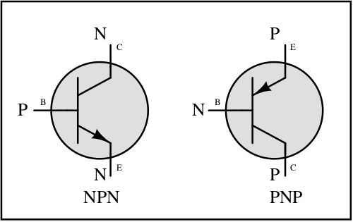
There are 2 types of BJT based on junction profile :
BJT symbol

In BJT, the 3 terminals are named as follows :
- Emitter (E)
- It is the terminal that emits the majority of charge carriers.
- Majority charge carriers in the case of NPN BJT are electrons. In case of PNP BJT, majority charge carriers are holes.
- It emits the charge carriers only if emitter-base (base-emitter) p-n junction is forward biased.
- Base (B)
- It is the controlling terminal which determines how much current should flow through emitter to the collector depending on voltage \(V_{BE}\).
- Collector (C)
- The majority of the current which is generated from the emitter is collected at collector terminal after bypassing base terminal.
The terminal with an arrow is the emitter terminal. The direction of the arrow is the direction of the current when the transistor is turned on. For NPN, the arrow is directed outwards of the device. In PNP, the arrow is directed inwards.
The middle terminal which goes to a perpendicular line is always the base. The terminal without the arrow is the collector terminal.
Modes of operation


| NPN | PNP | Notes | |||
|---|---|---|---|---|---|
| Modes | VBE | VBC | VEB | VCB | |
| Cut-off | <= 0 | <=0 | <= 0 | <= 0 | Open switch |
| Saturation | > 0 | > 0 | > 0 | > 0 | Closed switch |
| Forward active | > 0 | < 0 | > 0 | < 0 | Amplifier |
| Reverse-active | < 0 | > 0 | < 0 | > 0 | Not useful |
BJT as a switch (Cut-off and saturation region)
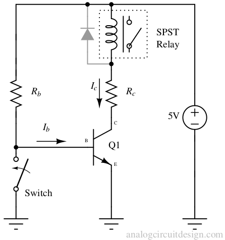
When BJT is used as a switch, the control terminals are Base-Emitter junction. The controlled terminals are Collector-Emitter junction.

In cutoff region \(V_i = 0\) and due to this \(V_{BE}\), \(I_c\) and \(I_b\) are zero. Because \(I_c\) is zero, \(V_o\) is pulled up to VCC. To visualize cutoff region, we can assume that the transistor is absent. In practical circuits, having \(V_i < 0.5\text{V}\) can push the transistor in cut-off region. We use cutoff region when we require an open-switch or we need to pull up \(V_o\) to VCC.

In saturation region, the transistor is supposed to fully turn on such that \(I_c\) becomes very high and pulls down \(V_o\) to ground. To get into saturation region, it is required to get \(V_i > 0.8\,\text{V}\). In that case \(V_{BE} \simeq{} 0.7\,\text{V}\), and \(I_b = (V_i – 0.7)/R_b\). We use saturation region when we require a closed-switch or there is a need to pull down \(V_o\) to ground. Practically, \(V_i\) is much higher than \(0.7\,\text{V}\) on the order of few volts. To limit the base terminal current, \(R_b\) is used. Also, the output \(V_o\) doesn’t touches ground but saturates near \(V_{ce(sat)}\).

As an example, BJT is often used to power the relay input. In place of the relay, we can use LED, motor, etc. When switch is closed, \(V_{BE} = 0\) so, \(I_b = I_c = 0\). The SPST relay is open because the inductor is de-energized. When the switch is open, the base current \(I_b\) starts flowing such that \(V_{BE} = 0.7\,\text{V}\). If the base current is flowing, the collector current will also flow which will energize the inductor in the SPST relay. Then the SPST relay will be closed.
If \(R_b = 0\), and switch is open, then \(V_{BE} = 5V\). In this condition base-emitter junction will be destroyed due to excessive current. So, it is required to limit the current to datasheet specifications by adding a minimum \(R_b\) in the base path.
In 2N3904, while in saturation, \(I_B = 5\,\text{mA}\) for \(I_C = 50\,\text{mA}\). So, value of \(R_B\),
$$R_B = \cfrac{5\,\text{V}-0.7\,\text{V}}{5\,\text{mA}}$$
$$R_B = 860\,\Omega{}$$
$$R_C = \cfrac{5\,\text{V}-0.2\,\text{V}}{50\,\text{mA}}$$
$$R_C = 96\,\Omega{}$$
BJT as an amplifier (Forward active)
When using BJT as an amplifier, it is important to power up (bias) the BJT for significant gain. We make sure that \(0.6\,\text{V}<V_{BE}<0.85\,\text{V}\) and \(V_{CE} > V_{CE(sat)}\). Usually, BJT is a current/voltage-controlled current device. Means output I-V characteristic suggests that output current remains fairly constant over a large range of output voltage. The output current depends only on the input voltage \(V_{BE}\) and current \(I_B\). So, whenever using BJT, current gain matters. This current gain can be converted to voltage gain by flowing the current through a resistor. In cut-off and saturation mode, the current gain is zero.
In forward-active mode, the principle relation between collector current and base-emitter voltage is :
$$I_C = I_S.\left[\exp{\left(\cfrac{V_{BE}}{V_t}\right)}-1\right]$$
It is observed that in real BJTs, output current \(I_C\) is affected by output voltage \(V_{CE}\) also. However affect is not as strong as input voltage \(V_{BE}\). To take into account the effect,
$$I_C = I_S.\left[\exp{\left(\cfrac{V_{BE}}{V_t}\right)}-1\right]\left(1+\cfrac{V_{CE}}{V_A}\right)$$
\(V_A\) is called the early voltage and usually a large number. That is why the effect of \(V_{CE}\) on \(I_C\) is low in comparison to \(V_{BE}\).
There are 2 important graphs/data (I-V characteristic) we need to check before choosing a DC bias circuit of a BJT :
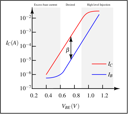
- \(I_c\), \(I_b\) vs. \(V_{BE}\)
- This graph tells us the optimal range of \(V_{BE}\) where \(\beta{}\) (current gain) is maximum. Usually with \(0.6\,\text{V} < V_{BE} < 0.85\,\text{V}\), \(\beta{}\) remain constant. Outside this region, \(\beta{}\) starts falling because of high base current or high level injection, so not very useful as an amplifier. Remember, while measuring the output current,\(V_{CE}\) is held constant using a voltage source at 1V.
- This is the input I-V characteristics plot. It is also called the Gummel plot.
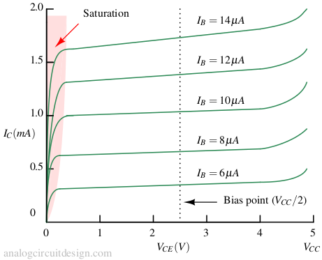
- \(I_c\) vs. \(V_{CE}\)
- This graph tells about the small-signal output resistance (i.e., \(V_A/I_C\)).
- Also, it tells us the region where saturation can happen. Remember, we avoid saturation in the amplifier because gain at saturation is zero.
- It is also called the output I-V characteristics plot.
Input I-V characteristics (Gummel plot)

Output I-V characteristics

In forward active region, there exist an important relationship :
$$I_B = \cfrac{I_C}{\beta{}}$$
Also, there exists another relationship that is valid in all modes of operation,
$$I_E = I_C+I_B$$
Therefore in forward active region,
$$I_B = \cfrac{I_E}{1+\beta{}}$$
