Transistors
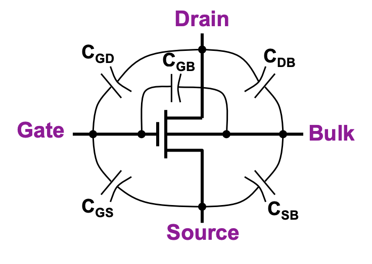
MOSFET parasitic capacitances are unintended capacitances formed between the gate, drain, source, and body due to device structure and junctions.

A transistor is a semiconductor device used to amplify or switch electronic signals, forming the building block of modern electronic circuits.

A power MOSFET is a high-current, high-voltage MOSFET designed for efficient switching and amplification in power electronics circuits.

An IGBT is a semiconductor device that combines the high input impedance of a MOSFET with the low conduction loss of a bipolar transistor, used for switching and amplification.
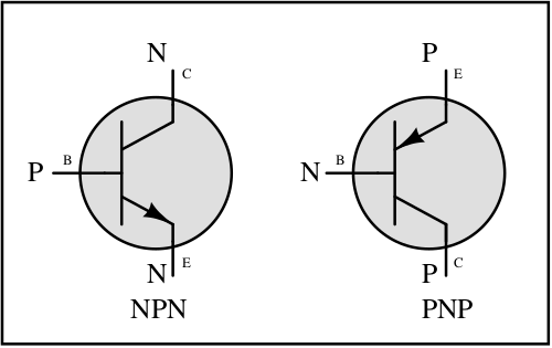
An NPN transistor is a bipolar junction transistor where a layer of P-type material is sandwiched between two N-type layers, allowing current amplification and switching.
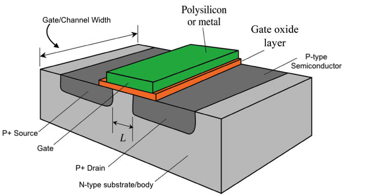
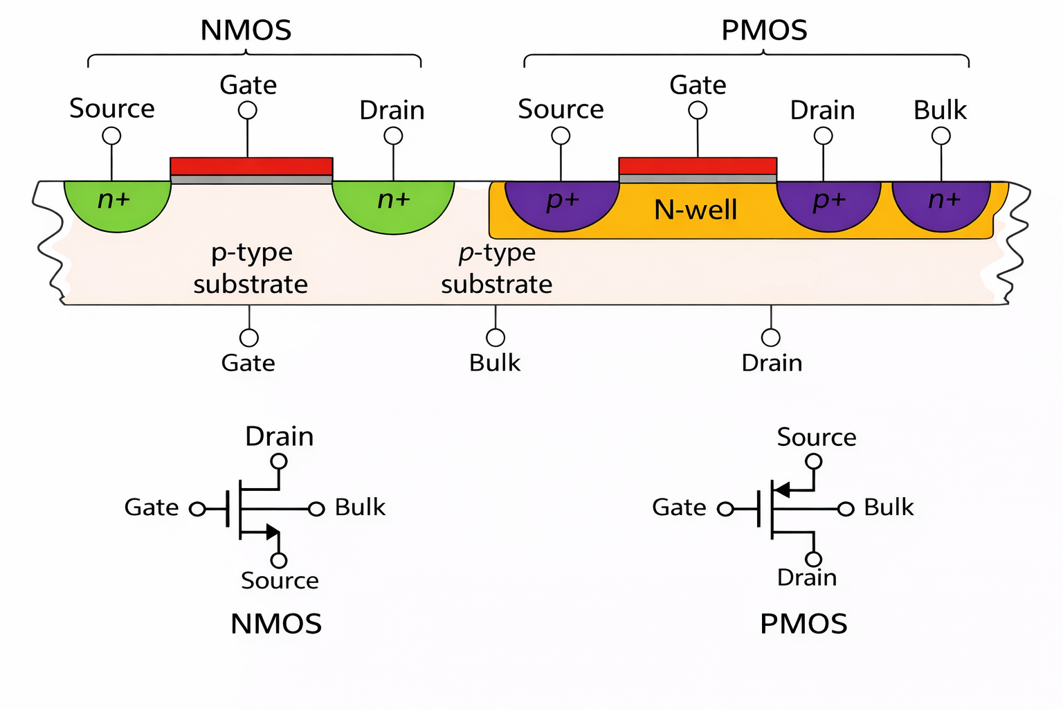
A P-channel MOSFET is a type of MOSFET where current flows through a channel of holes controlled by a negative voltage applied to the gate.

A JFET is a voltage-controlled semiconductor device where current flows through a channel controlled by the voltage applied to the gate terminal.
CMOS fabrication flow involves a series of steps like oxidation, photolithography, doping, etching, and metallization to create integrated circuits using complementary MOS transistors.

Latch-up is a failure condition in CMOS circuits where a low-impedance path forms between the power supply rails, causing excessive current and potential device damage.

A MOSFET (Metal-Oxide-Semiconductor Field-Effect Transistor) is a voltage-controlled transistor used for switching and amplification in electronic circuits.
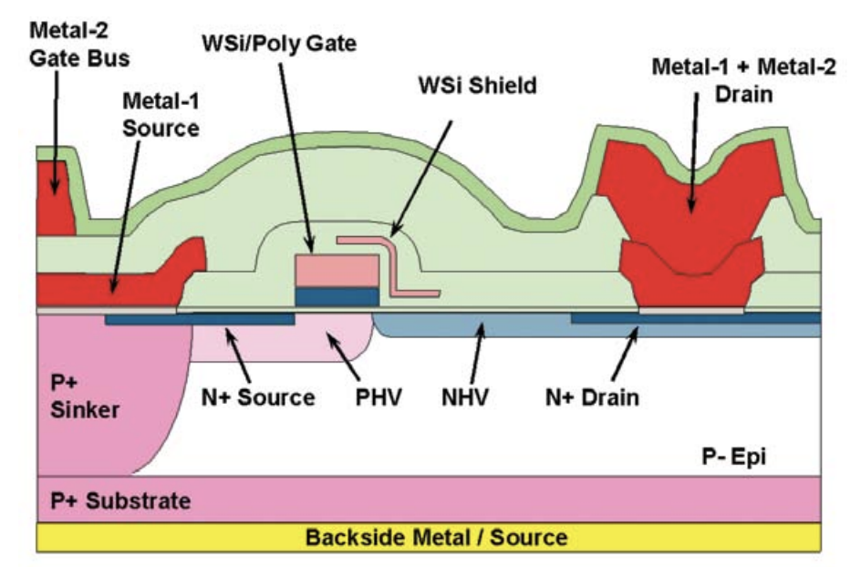
LDMOS (Laterally Diffused MOSFET) is a high-power MOS transistor optimized for RF and power amplification with low on-resistance.

A floating gate MOSFET is a type of transistor with a gate isolated by an insulator, capable of storing charge to retain information even without power.
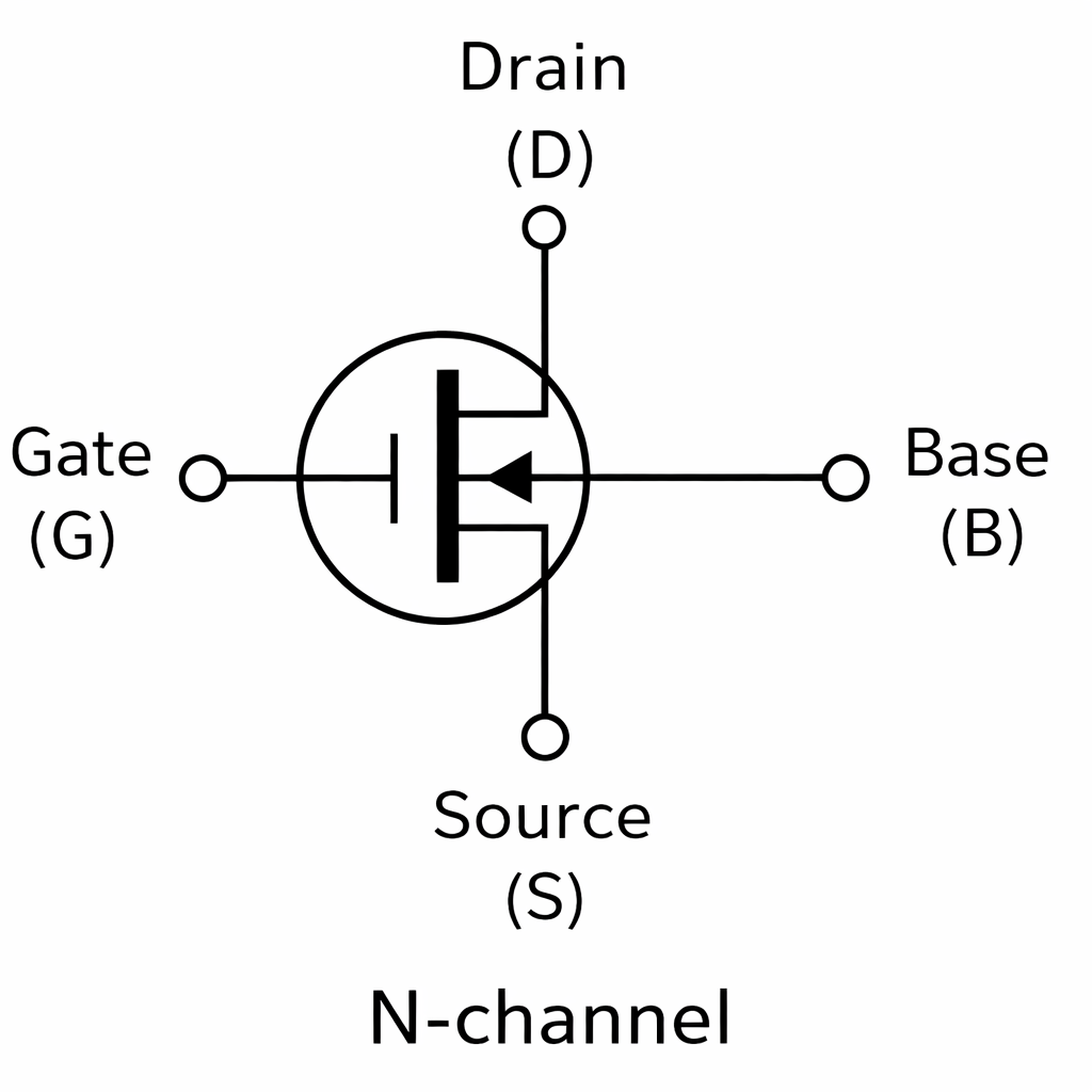
An N-channel MOSFET is a type of MOSFET where current flows through a channel of electrons controlled by a positive voltage applied to the gate.

A MOSFET circuit model represents the behavior of a MOSFET using equivalent circuits for analysis of voltage, current, and small-signal performance.
A PNP transistor is a bipolar junction transistor where a layer of N-type material is sandwiched between two P-type layers, allowing current amplification and switching.
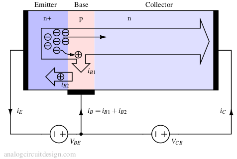
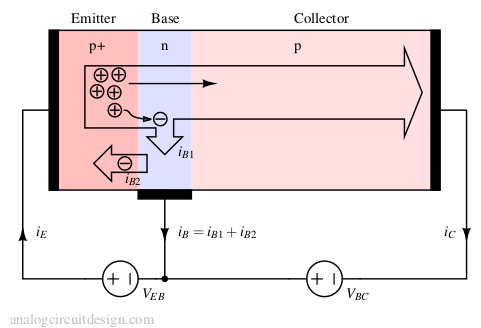
A bipolar junction transistor (BJT) is a semiconductor device used to amplify or switch electronic signals, consisting of two junctions and three terminals – emitter, base, and collector.
