CMOS Fabrication Process
The fabrication of CMOS (Complementary Metal-Oxide-Semiconductor) is a complex, multi-step process that integrates both N-channel (NMOS) and P-channel (PMOS) transistors on a single silicon substrate.
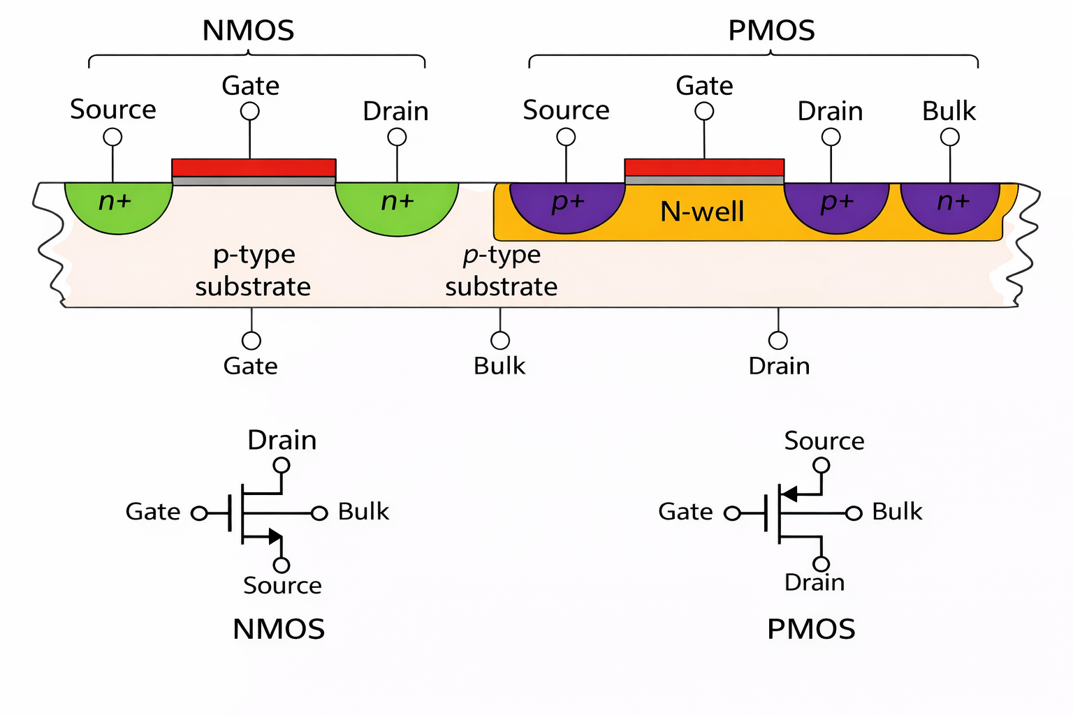
The most common CMOS manufacturing method is the N-well inside a P-type substrate. It is competitively priced though prone to latch-up in radiation environment (e.g., space applications). Another process is Twin-tub in a SOI which is a expensive process but avoids latchup in radiation environment.
What is CMOS technology
In CMOS technology, both n-type and p-type metal-oxide-semiconductor field-effect transistors (MOSFETs) are used together in a complementary fashion. This means that for every n-type MOSFET, there is a corresponding p-type MOSFET, forming a complementary pair.
Combining these two types of transistors allows for low power consumption and high noise immunity. CMOS circuits consume power only when they switch states, which means they are very efficient in power usage. This makes CMOS technology ideal for portable devices, where battery life is crucial.
CMOS technology also offers high noise immunity, meaning it can tolerate noisy or degraded input signals without a significant impact on the circuit's performance. This is because CMOS circuits use transistors with a large voltage gain and high input impedance, which helps reduce noise's impact. Furthermore, CMOS technology allows for the integration of a large number of transistors on a single chip, enabling the development of complex integrated circuits.
This integration density has been a driving force behind the advancements in the field of microprocessors and other digital ICs. It is a widely used technology for constructing integrated circuits (ICs) and is especially prevalent in the field of digital logic design. CMOS technology is used to build processors, memory chips, and various other electronic devices.
Manufacturing steps of N-well process
CMOS (Complementary Metal-Oxide-Semiconductor) fabrication involves a series of steps to create integrated circuits (ICs) on a silicon wafer. Some steps are mentioned below in a simplified way:
Base (substrate) preparation
The process begins with preparing a silicon wafer, which serves as the base material for the ICs. The wafer is cleaned to remove impurities and is polished to ensure a smooth surface.

Oxidation to create SiO2 layer
The wafer undergoes oxidation, where a thin layer of silicon dioxide (SiO2) is grown on its surface. This layer acts as an insulating material and provides electrical isolation between different components.
Etching to create active areas
This step applies a photoresist layer of photosensitive material to the oxide layer. The wafer is exposed to UV light through a mask containing the desired circuitry pattern. The UV light chemically alters the photoresist, creating a patterned layer.
Etching is performed to remove the exposed portions of the oxide layer. This is typically done using a chemical etchant that selectively removes the oxide, leaving behind the patterned areas protected by the photoresist.
Active areas: These are the areas where active components are created, like NMOS, PMOS, PNP, and NPN.
Trench filling with oxide

N-well implant
N-type material is introduced in the p-epi region to N-well where PMOS will be created. This is done with the help of an N-well mask.
P-well implant
P-type material is introduced in the p-epi region to the P-well, where NMOS will be created. This is done with the help of a P-well mask.
Gate patterning and self-aligned source/drain creation
The gate-insulating layer (SiO2) is formed near the beginning of the process. Then the gate is deposited and patterned on top. Then the source drains are doped (for poly-silicon, the gates are doped simultaneously).
Please note that source/drain patterning does not require a separate source/drain mask. The source and drain are created in the area where Gate is not patterned. The gate itself acts as a mask. However, separate masks (N-well and P-well) are required to dope PMOS and NMOS source/drain regions, respectively.
Usually, the source and drain are doped using a process called ion implantation. The wafer is heated to a high temperature in a process known as annealing. This helps to activate the dopants and repair any damage caused during the ion implantation step.

Via/Contact patterning
Openings are made in the insulating layers, exposing the underlying transistors and metal layers. These openings are filled with metal (usually tungsten), creating contacts and vias that provide electrical connections between the various components.
Formation of interconnects by deposition of metal (BEOL)
Once the transistor structures are formed, metal layers (such as aluminum or copper) are deposited on top of the wafer, called the BEOL (Back end of the line) process. These metal layers serve as interconnects, allowing electrical connections between different components on the chip.
Steps of the BEOL:
- Silicidation of source and drain regions and the polysilicon region.
- Adding a dielectric (first, the lower layer is pre-metal dielectric (PMD) – to isolate the metal from silicon and polysilicon), CMP processing it
- Make holes in PMD, and make contacts in them.
Add metal layer 1 - Add a second dielectric, called the inter-metal dielectric (IMD)
- Make vias through the dielectric to connect lower metal with higher metal.
- Vias are filled by Metal CVD (Chemical vapor deposition) process.
- Repeat steps 4–6 to get all metal layers.
- Add a final passivation layer to protect the microchip.
Post fab-out process
The fabricated ICs are tested for functionality and performance. They are then separated into individual chips and packaged into appropriate housing, which includes leads or pins for external connections.