Insulated gate bipolar transistor (IGBT)
The Insulated Gate Bipolar Transistor (IGBT) is a three-terminal power semiconductor device that combines that inherits the advantages of BJTs' output switching/conduction characterisitics and MOSFETs' infinite input resistance. Having infinite input resistance makes it a voltage controlled device. It is widely used in high-power applications, including motor drives, power converters, inverters, and amplifiers.
MOSFET vs IGBT
The IGBT1 is considered to be the optimal combination of the benefits of a MOSFET gate and BJT current output. Some key differences are listed below:
| MOSFETs | IGBT | |
|---|---|---|
| Switching Frequency | Better than IGBTs | Worse than MOSFETS |
| Suitability as switch | Highly suitable due to almost zero off-state current | Not suitable due to non-zero off-state current |
| Die size | Larger for same output resistance | Smaller for same output resistance |
| Capacitance | Higher capacitance for same output resistance | Smaller capacitance for same output resistance |
| Driving circuits | Due to higher capacitance, need more switching current | Due to lower capacitance, need less switching current |
| Digital circuits and Scalability | Highly favorable for digital circuits due to negligible off-current and highly scalable | Not favorable for digital circuits because IGBTs are optimised for high-power applications and not very scalable as MOSFET |
| Noise contribution type | Thermal noise and Flicker noise | Shot noise, Thermal noise and Flicker noise |
| High power circuits suitability | Less suitable to high channel resistance. Capacitance increases to decrease channel resistance | Low channel resistance. Capacitances are less than MOSFETs for similar breakdown voltages |
Circuit symbols of IGBTs
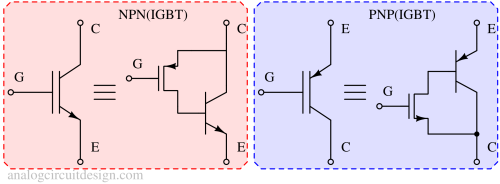
The symbol of an Insulated Gate Bipolar Transistor (IGBT) is typically represented as follows:

In the symbol of NPN (IGBT), the vertical line on the \left side represents the Gate (control terminal), the parallel line adjacent to the Gate is Base, and the vertical line on the top side represents the collector. The arrow pointing out of the base region represents the Emitter.
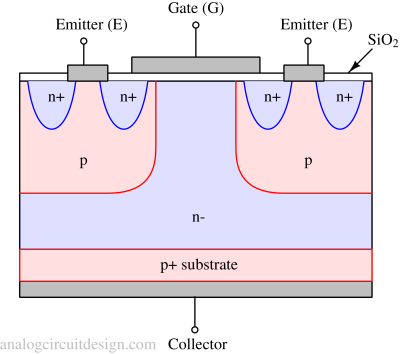
Structure of IGBTs
The structure of an IGBT consists of a vertical arrangement of four layers: a P-type substrate, an N-type collector, a P-type base region, and an N-type drift region. The base region is connected to the gate terminal through a thin layer of insulation, usually made of silicon dioxide (hence the name "Insulated Gate" Bipolar Transistor). This insulated gate structure allows for efficient control of the device.

Advantages of IGBTs
The IGBT offers several advantages over other power devices. It can handle high currents and voltages while providing good thermal stability. Additionally, IGBTs have a built-in diode (called a "freewheeling diode") in parallel with the collector-emitter path, which helps with the current flow during the switching transitions and prevents damage due to the reverse current.
Also, it offers greater power gain than the standard bipolar-type transistor combined with the higher voltage operation and lower input losses of the MOSFET.
The IGBT has a much lower “on-state” resistance, RON, than an equivalent MOSFET. This means the I2R drop across the bipolar output structure for a given switching current is much lower. The forward blocking operation of the IGBT transistor is identical to a power MOSFET.
Modes of operation
On-state
When a positive voltage is applied to the gate terminal with respect to the emitter, a channel is formed between the N-type drift region and the P-type base region. This allows current to flow from the collector to the emitter, similar to a BJT. The conductivity of this channel is controlled by the gate voltage, enabling precise control of the IGBT's on-state characteristics.
Off-state
When the gate-emitter voltage is zero or negative, the channel is depleted, and the IGBT blocks current flow between the collector and emitter. It exhibits a high voltage-blocking capability similar to a MOSFET.
Applications of Insulated gate bipolar junction transistor (IGBT)
The IGBT is a transistor ideal for high-voltage, high-current applications. Available with a voltage rating ranging from 400 V to 2000 V and a current rating ranging from 5 A to 1000 A, the IGBT is widely used for industrial applications such as inverter systems and uninterruptible power supplies (UPS), consumer applications such as air conditioners and induction cookers, and automotive applications such as electric vehicle (EV) motor controllers.