Transistors basics
A modern transistor is an electronic device that uses a semiconductor to amplify or switch electronic signals. It is usually a three-terminal device, where the current through two terminals is controlled using the voltage at the third terminal. Modern transistors are used to create microprocessors, cellular infrastructure, memory devices etc.
History of Transistors
The modern transistor was invented in 1947 by John Bardeen, Walter Brattain, and William Shockley at Bell Labs, revolutionizing electronics. The first was a point-contact transistor, followed by Shockley's junction transistor in 1948. Transistors replaced bulky and power-hungry vacuum tubes, enabling smaller, energy-efficient machines. In the 1950s, commercial production began with germanium transistors. Silicon transistors, introduced in the late 1950s, became dominant due to the property of silicon to form silicon dioxide quickly. The 1960s saw integrated circuits incorporating multiple transistors in a single substrate, sparking the microelectronics revolution.
Working Principle of transistors
Most transistors have three terminals. We can identify them as control terminal (Tctrl), Output terminal (Tout) and Reference terminal (Tref). Usually, the voltage difference between Tctrl and Tref is used to control the amount of current flowing through Tout to Tref. A transistor can be used in two ways :
- Amplifier (e.g., voltage controlled current source)
- Switch
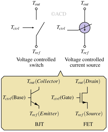
Transistor as an amplifier
Most transistors, whether BJTs or FETs, act as voltage-controlled current sources. In BJTs, we apply voltage at the base terminal (emitter grounded), which controls the collector current. In FETs, the control voltage is applied at the gate terminal (and source grounded), which controls the current through the drain terminal.
Transistor as a switch
The amplification property of a transistor can be used to create a switch. If the control voltage is high enough, it will saturate the output of the transistor to supply voltage. If the control voltage is low (near zero), the transistor output will saturate the ground. A transistor is used as a switch to turn a circuit on or off. This can create logic in digital circuits or control electronic components in a home appliance or an automobile.
Types of Transistors
The fundamental types of transistors are :
Bipolar Junction Transistors (BJTs)
BJTs have three terminals: Base, Emitter, and Collector. They form two important junctions: the base-emitter junction and the base-collector junction. The biasing of these junctions decides the operation, so they are called junction transistors.
The BJT terminals are called Base, Emitter, and Collector. The emitter is the terminal from which the majority charge carriers enter the transistor. The emitter region is heavily doped to inject carriers into the base. The collector is the terminal from which the majority charge carriers leave the transistor. The collector region is moderately doped and larger in size to collect carriers from the emitter. The base is the control terminal where voltage is applied to control the flow of charge carriers in the channel. The base region is thin and lightly doped to control the carrier flow between the emitter and collector.
In a BJT, mobile charge carriers are generated in the emitter-base junction by forward biasing it. Most (β/1+β) of them are absorbed into the collector region before some carriers (1/1+β) reach the base terminal. β is called the current gain factor, which is the ratio of collector current (IC) and base current (IB).
They are called bipolar because their operation involves both types of charge carriers: electrons (negative charge) and holes (positive charge).
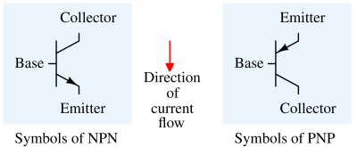
There are two types of BJTs :
- NPN : The layers/terminals are arranged as N-type (Emitter) - P-type (Base) - N-type (Collector).
- PNP : The layers/terminals are arranged as P-type (Emitter) - N-type (Base) - P-type (Collector).
Field Effect Transistor (FET):
The term “field” refers to the electrical field that affects the conductivity of the channel through which charge carriers can flow. A control voltage (applied at the Gate terminal) affects the concentration of charge carriers in the channel.
The terminals of Field-Effect transistors are called Gate, Source, and Drain. The source is the terminal from which the majority charge carriers enter the channel. The Drain is the terminal from which the majority charge carriers leave the channel. The gate is the control terminal where voltage is applied to control the flow of charge carriers in the channel.
There are primarily three types of Field Effect Transistors (FETs) :
Junction Field Effect Transistors (JFET)
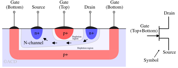
A JFET (Junction Field Effect Transistor) is the simplest form of FET that uses a reverse-biased PN junction to control the effective channel width. The reverse bias voltage of the PN junction controls the depletion width inside the channel; hence, it controls the channel width. Since the gate-source junction is reversed-biased, the gate current is negligible. It is much less than BJT’s base current.

There are two types of JFET :
- N-channel JFET - The current travel through an N-type channel. The control gates are P-type.
- P-channel JFET - The current travel through a P-type channel. The control gates are N-type.
Metal Oxide Semiconductor FET (MOSFET)
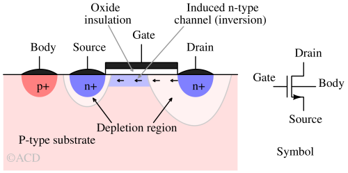
A thin oxide layer isolates the gate terminal from the channel, allowing MOSFETs to have no (zero) gate current at DC. When a gate voltage is applied, the channel is inverted. Inversion of the channel means if the channel was originally P-type, the gate voltage attracts electrons from the channel to form a thin N-type region. This inversion forms a bridge between the source and drain to allow current flow. For understanding, the body terminal can be ignored for now and safely shorted to source terminal.

There are two types of MOSFETs :
- N-channel MOSFET - The current traveling through an induced N-type channel. The original channel is P-type. The source and drain are N-type. The control gates are made using Polysilicon.
- P-channel MOSFET - The current traveling through an induced P-type channel. The original channel is N-type. The source and drain are P-type. The control gates are made using Polysilicon.
FinFETs
 A FinFET is a field-effect transistor (FET) type featuring a thin, vertical, three-dimensional rectangular-shaped fin serving as the channel. The channel is wrapped by the gate on three faces. In contrast, a fully planar design has a channel below the gate, and the gate controls only one face of the channel. The extreme ends of the channel serve as the source and the drain. In FinFET, the three-dimensional design of the channel increases the surface area between the gate and channel, improving control over the channel's electric state and reducing leakage compared to planar FETs.
Comparison between BJTs and FETs
Following is the comparison between BJT and FET. Assuming both transistors have an output current Iout (BJT’s collector current and FET’s drain current):
| BJT | FET | |
|---|---|---|
| Input current | Iout/β | 0 |
| Transconductance (gm) | Iout/Vt | < Iout/Vt |
| Dominant noise source | Shot noise | Flicker and thermal noise |
| Flicker noise | Very less (10x lower than MOSFET) | MOSFET’s flicker noise is higher than BJTs (could be 10x higher). JFET’s flicker noise is lower than BJTs. |
| Suitability for Very Large Scale Integration (VLSI) | It is not suitable because of the non-zero input current. Very high standby current. | MOSFETs and FinFETs are suited for large scale integration (beyond sub-100nm). JFETs are less suited for sub-100 nm integration due to leakage and less speed. |
| Precision | Achieves better precision. | Has worse precision than BJTs. Chopping allows very high precision. |
| Switching speed | It is slower because of charge storage in the base region. | Typically, it is faster due to the absence of charge storage. |
| Circuit design complexity | High | Relatively low |
| Thermal Stability | Prone to thermal runaway, especially in power applications. | Better thermal stability means performance is less affected by temperature changes. |
| Reliability | It is more reliable because everything is PN junction. | It is less reliable because of a thin oxide layer at the Gate. |
The key difference between BJTs and FETs is that BJTs offer higher gain and bandwidth for the same current, along with better noise performance and superior output current drive capability. However, their main drawbacks include a non-zero input current requirement and the potential for phase reversal.
Some other types of transistors
Unijunction transistor (UJT)
A unijunction transistor consists of a \bar of N-type silicon with a P-type junction at its center.

The emitter current versus voltage characteristic curve of a unijunction transistor shows that as VE-B1 increases, the emitter current IE rises to the peak point IP. Beyond this peak, the voltage decreases while the current increases, creating a negative resistance region. The voltage reaches its minimum at the valley point when the current is IV. At this point, the resistance of RB1, known as the saturation resistance, is at its lowest value.
HBT
A heterojunction bipolar transistor (HBT) is a variation of a bipolar junction transistor (BJT) in which different semiconductor materials are used for the emitter and base regions, forming a heterojunction. In a homojunction NPN device, the holes going from base to emitter must be reduced to increase the current gain (β). To do that, base doping is reduced. By doing this, β is increased, but base-width modulation increases, reducing the Early voltage (VA). HBTs solve this problem and provide higher current gain and higher Early voltage together.
HEMT
High-electron-mobility transistors (HEMTs or HEM FETs) are field-effect transistors that leverage a heterojunction formed by materials with differing band gaps. These devices provide superior performance in high-frequency applications.
Important BJT parameters
To design a circuit with BJT (NPN or PNP), we should know the following parameters from the datasheet:
Current gain (hfe or β)
The current gain (hfe or β) at the desired load current (Ic). This will help us derive the current limit resistor’s value at the base. Usually, it is 100 for very common transistors.
VCE,min (Collector saturation voltage)
The minimum collector-emitter voltage (VCE,min) is required to maintain the collector current, which falls rapidly below this voltage.
BVCEO (Breakdown voltage)
The maximum collector-emitter voltage, also called the Breakdown voltage of the CE junction (BVCEO).
IC,max (current-rating)
This shows the transistor’s maximum current handling capability. Some transistors are designed to carry only signals, meaning the current rating would be low. Some transistors are designed to carry power, meaning the current rating would be higher.
FT,max (transition-frequency)
FT symbolises the maximum frequency achievable for a given current-density (current for a fixed size of transistor). FT,max indicates the maximum achievable frequency across the current densities.
VBE,on
This is the required base-emitter voltage to turn on the transistor. It is usually 0.7V (VBE), but it can go as high as 1V. Applying more than 1V can permanently destroy the transistor.
Some popular discrete NPN transistors
| Sr. No | Transistor name | FT | hfe | BVCEO | VCE, min @ 10mA | IC,max |
|---|---|---|---|---|---|---|
| 1 | 2N3904 | 300MHz | 100 | 40V | 0.2V | 200mA |
| 2 | 2N2222 | 300MHz | 100 | 40V | 0.3 | 600mA |
| 3 | BC547 | 300MHz | 110 | 45V | 0.09V | 100mA |
| 4 | BC817 | 100MHz | 100 | 45V | 0.7 | 500mA |
| 5 | BC337 | 210MHz | 100 | 45V | 0.7 | 800mA |
Some popular discrete PNP transistors
| Sr. No | Transistor name | FT | hfe | BVCEO | VCE, min @ 10mA | IC,max |
|---|---|---|---|---|---|---|
| 1 | 2N3906 | 250MHz | 100 | 40V | 0.25V | 200mA |
| 2 | BC327 | 100MHz | 100 | 50V | 0.7V | 800mA |
| 3 | BD140 | 20MHz | 100 | 45V | 0.5V | 1.5A |
| 4 | BC807 | 100MHz | 100 | 50V | 0.7V | 500mA |
Important FET parameters
To design a circuit with FET (N-channel or P-channel), we should know the following parameters from the datasheet:
VGS(th)
It is the Threshold Voltage of the transistor. Above this voltage, the FET starts conducting. Below this voltage, the FET acts as an open circuit and has zero output current.
VGSS (Gate breakdown voltage)
This is the maximum voltage that could be applied at the gate terminal (gate-source in case of N-channel FET and source-gate in case of P-channel FET), which is the control terminal of the FET. This is usually lower than BVDSS. VGSS is generally less than 5V in integrated circuits and sometimes less than 1V. In discrete transistors, this voltage could be as high as 20V.
BVDSS (Drain breakdown voltage)
This is the maximum voltage which can be applied at the drain. Beyond this voltage, the transistor does an avalanche breakdown.
RDS,ON (On resistance)
It indicates the drain-source resistance when the transistor is turned-on.
ID,max (continuous drain current) at 25°C
When turned on, this is the transistor's maximum current-carrying capacity at 25°C.
Ton or Toff (Turn-on or turn-off time)
This indicates the speed of the FET when the gate is driven by sufficient current. Usually, it indicates how fast the drain current builds up and collapses, indicating the switching time.
Ciss (Input capacitance)
This shows the amount of parasitic capacitance at the gate. A higher Ciss value requires a powerful gate driver to achieve fast transients.
IGSS (gate-source leakage current)
The Ideal FET device has zero gate-source leakage current, but in reality, it ranges from a few pA to hundreds of nA. In most cases, this current can be ignored in FETs.
Popular discrete N-channel MOSFET
| Sr. No | Transistor name | VTH | BVDSS | RDS(on) | Ciss | VGSS | Ton / Toff | ID,max |
|---|---|---|---|---|---|---|---|---|
| 1 | 2N7002 | 1V | 60V | 1.2Ω | 20pF | 20V | 20ns / 20ns | 115mA |
| 2 | 2N7000 | 0.8V | 60V | 1.2Ω | 20pF | 20V | 10ns / 10ns | 200mA |
| 2 | IRFZ44n | 2V | 55V | 17.5mΩ | 1470pF | 20V | 12ns / 44ns | 49A |
| 3 | BSS138 | 0.8V | 50V | 3.5Ω | 27pF | 20V | 2.5ns / 20ns | 220mA |
| 4 | IRF540 | 2V | 100V | 77mΩ | 1700pF | 20V | 11ns / 53ns | 28A |
| 5 | BS170 and MMBF170 | 0.8V | 60V | 1.2Ω | 24pF | 20V | 10ns / 10ns | 500mA |
Popular discrete P-channel MOSFET
| Sr. No | Transistor name | |VTH| | |BVDSS| | RDS(on) | Ciss | VGSS | Ton / Toff | ID,max |
|---|---|---|---|---|---|---|---|---|
| 1 | BS250 | 1V | 45V | 14Ω | 60pF | 20V | 20ns / 20ns | 230mA |
| 2 | IRF9540 | 2V | 100V | 200mΩ | 1400pF | 20V | 16ns / 34ns | 19A |
| 3 | IRF4905 | 2V | 45V | 20mΩ | 3400pF | 20V | 18ns / 61ns | 74A |
How to use a BJT ?
The following sections discuss the basic circuits of NPN and PNP transistors used as switches:
Connection of an NPN transistor
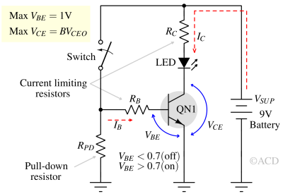
To turn on an NPN transistor, the base voltage must be at least 0.7V higher than the emitter voltage. A red LED needs at least 20mA to glow, so the collector current needs to be 20mA. At this collector current, transistor 2N3904 has a current gain (hfe or β) of 100. So, the current needed from the base terminal is IB = (IC/β) = 200uA. The base-to-emitter voltage needs to be at least 0.7V.
Value of RB (using KVL) :
$$R_B=\cfrac{V_{SUP}-V_{BE,on}}{I_B}=\cfrac{9-0.7}{200\mu{}\text{A}}$$
The collector voltage must also be higher than the emitter voltage by at least 0.5V (VCE, min). The voltage drop across the LED would be 1.8V (VLED). So, the voltage source VSUP should be at least 1.8V + 0.5V = 2.3V (VCE, min + VLED). Higher VSUP improves current gain (hfe) and speed. If a 9V battery is used for VSUP, we can calculate the value of RC.
Maximum value of RC (using KVL) :
$$R_C=\cfrac{V_{SUP}-V_{LED}-V_{CE,min}}{I_C}=\cfrac{9-1.8-0.5}{20\text{mA}}=335\Omega{}$$
A value of more than 335 Ω will crunch the VCE, resulting in less than the required current flowing through the LED. The VSUP voltage source should not exceed the breakdown voltage BVCEO (40V in the case of 2N3904).
Connection of a PNP transistor
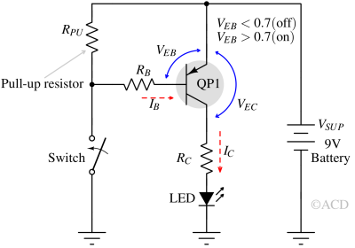 To turn on an NPN transistor, the base voltage must be at least 0.7V higher than the emitter voltage. A red LED needs at least 20mA to glow, so the collector current needs to be 20mA. At this collector current, transistor 2N3904 has a current gain (hfe or β) of 100. So, the current needed from the base terminal is IB = (IC/β) = 200uA. The base-to-emitter voltage needs to be at least 0.7V.
How to use a MOSFET ?
The following sections discuss the basic circuits of NMOS and PMOS transistors used as switches:
Connection of an NMOS transistor
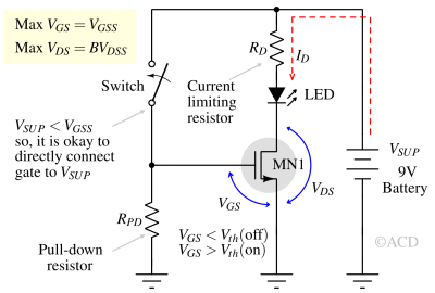
To operate NMOS as a switch, the gate is connected to one end of the switch, and the other is connected to the power supply. So, whenever the switch is closed, VGS is greater than the threshold voltage (VTH), and the FET (MN1) starts conducting, causing the LED to glow. The pull-down (RPD) resistor makes the gate voltage zero whenever the switch is opened. The current into the gate terminal is always zero (some nano amperes, in reality). RD is added to limit the current to near 20mA, preventing LED destruction. The high voltage drop across RD reduces the VDS of the transistor to just a few millivolts, significantly limiting the current flow.
Value of RD :
Since the VGS equals 9V when the switch is closed, the current MN1 can provide way more than 20mA. According to the datasheet 2N7002, the current would be more than 1A if VDS is over a volt. The output terminal behaves as a resistor with an RDS(on) value when VGS exceeds VDS + VTH (VTH ~ 1V and VDS < 1V). The value of RDS(on) is 1.2Ω for 2N7002. VLED is again 1.8V for a red LED. So, using KVL to derive the value of RD :
$$V_{SUP}-I_DR_D-V_{LED}-I_DR_{DS(on)}=0$$
$$R_D=\cfrac{V_{SUP}-V_{LED}}{I_D}-R_{DS(on)}=\cfrac{9\text{V}-1.8\text{V}}{0.02\text{A}}-1.2\Omega{}\simeq{}360\Omega{}$$
If we observe, we don’t have an RB like the one we had in the BJT transistors mentioned above. This is because the gate current is zero in FET devices. In BJTs, due to IB, the large RB creates a massive voltage drop from the large supply voltage, protecting the base-emitter junction. In the case of FETs, the entire supply voltage would come at the gate due to the pull-up resistor. If the gate terminal can tolerate only 20V but the supply voltage is 40V, we need additional circuits, as shown below.
Connection of a PMOS transistor
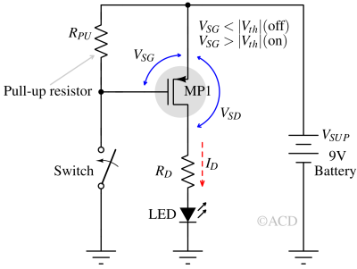
To operate PMOS as a switch, the gate is connected to one end of the switch, and the other is connected to the ground. When the switch is closed, the source-gate voltage (VSG) exceeds the threshold voltage (VTH), causing the PMOS transistor (MP1) to conduct and the LED to light up. A pull-up resistor (RPU) ensures that the source-gate voltage (VSG) becomes zero when the switch opens. The gate current is negligible, typically in the range of a few nanoamperes.
A resistor (RD) is included to limit the current to approximately 20mA, protecting the red LED from damage. The significant voltage drop across RD reduces the transistor's VDS to just a few millivolts, constraining the current flow.
Value of RD :
The output terminal behaves as a resistor with a value of RDS(on) when VGS is higher than VDS + VTH (VTH ~ 1V and VDS < 1V). The value of RDS(on) is 14Ω for BS250. VLED is again 1.8V for a red LED. So, using KVL to derive the value of RD :
$$V_{SUP}-I_DR_D-V_{LED-I_DR_{DS(on)}}=0$$
$$R_D=\cfrac{V_{SUP}-V_{LED}}{I_D}-R_{DS(on)}=\cfrac{9\text{V}-1.8\text{V}}{0.02\text{A}}-14\Omega{}=346\Omega{}$$
If VSUP is higher than the maximum source-gate voltage (VGSS) that can be applied, we must protect the gate using Zener protection. The Zener protection circuits maintain a maximum VZ voltage across the source gate, saving the FET MP1 from destruction.
Applications of Transistors
- Amplifiers in audio systems.
- Switches and logic gates in digital circuits.
- Core components in integrated circuits (ICs) and microprocessors.
- Power regulation in electronic devices.
Advantages of Transistors against vacuum tubes
- The compact size makes them easy to integrate
- Discrete transistors are lightweight
- High energy efficiency due to low power consumption
- Durability and reliability