Junction Field Effect Transistor (JFET)
Junction Field-Effect Transistors (JFETs) are three-terminal semiconductor devices used in electronics to provide a robust high impedance with lower noise. JFETs act as voltage-controlled current sources and voltage-controlled switches. The control terminal is called the Gate, while the current flows through Source and Drain terminals. JFETs operate in depletion mode, meaning the channel is already present when there is zero control voltage (VGS = 0). Applying a reverse bias voltage at the Gate-source terminal reduces the current.
JFETs are used as the input stage of BJT amplifiers to provide very high input impedance, low flicker noise, and input current noise at a decent power budget. Examples of such amplifiers are OPA828, ADA4817, etc.

Construction of JFET
A JFET comprises three main terminals: source, drain, and gate. Depending on the type of semiconductor material used, the construction can be categorized into N-channel and P-channel JFETs.
- N-channel JFET: In an N-channel JFET, the channel is made using N-type semiconductor material doped with donor impurities (e.g., Phosphorus, Arsenic, Antimony, and Bismuth). Ohmic contacts with N+ doping are placed at both ends of the channel to serve as the source and drain connections. The gate terminals are made from P-type material, forming two PN junctions with the N-channel.
- P-channel JFET: In contrast, in a P-channel JFET, the channel is made using P-type semiconductor material, which is doped with acceptor impurities (e.g., Boron, Aluminum, and Gallium). Ohmic contacts with P+ doping are placed at both ends of the channel to serve as the source and drain connections. The gate terminals are made from N-type material, forming two PN junctions with the P-channel.
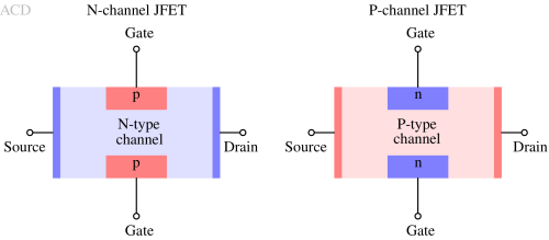
A simplified diagram is shown above. The channel is sandwiched between the gates. Usually there are two gates in a JFET. Both of them are connected together in reality to form a single gate terminal.
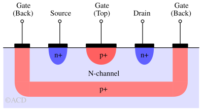
In Figure 3, an actual construction of JFET is shown. There are two gate terminals. One is a top-gate terminal, and another is a back-gate terminal. The back-gate terminal is buried under the channel. The back gate is bent upwards, contacted at the top, and shares a large surface area with bulk. The source and drain terminals are symmetric. In an N-channel JFET circuit, the terminal with the highest potential is identified as the drain, while the terminal with the lowest potential is identified as the source terminal.
Symbols of JFETs
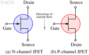
- N-channel JFET symbol : The symbol features an arrow on the gate pointing toward the channel. The significance of the arrow is that if gate-source junction is forward biased, the current will flow into the gate towards the channel. In N-channel JFETs, electrons are the charge carriers which originate from source. So, the direction of current flow is from drain to source in N-channel JFET.
- P-channel JFET symbol : The symbol has an arrow on the gate pointing away from the channel, signifying that if gate-source PN junction is forward biased, the current will flow out of the gate. In P-channel JFETs, holes are the charge carriers which originate from source. So, the direction of current flow is from source to drain in P-channel JFET.
Working principle of JFET
Let's understand the workings of a JFET by drawing an analogy to a water pipe. When there is no obstruction, water flows smoothly through the water pipe. However, if the water pipe is squeezed, the water flow decreases. A JFET operates on the same principle. In this analogy, the water pipe represents the JFET, and the water flow corresponds to the current. The current can be controlled by shaping the current-carrying channel as needed using a control voltage.
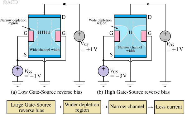
In a JFET, the width of the conduction channel between Source-Drain is controlled by the depletion region of the reverse biased Gate-Source junction. This modulation of the conduction channel's width results in transistor behavior.
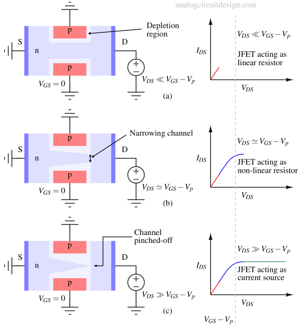
In Fig 5, the simplified operation of N-channel JFET is explained. The gates are p-type (red), and the channel is n-type (blue). The light shade of blue region represents the depletion region. The darker blue area shows the contacts for the drain and source.
In Fig 5 (a), the Gate-Source voltage applied is -1V. The Drain-Source voltage is 1V. Near the drain terminal, the effective reverse bias for the Gate-Drain PN junction is 2V. Near the source region, the effective reverse bias for the Gate-source PN junction is 1V. So, the depletion width is higher near the drain and lower near the source terminal. That is why the depletion region shape seems to taper down from drain to source. In the PN junction, the width of the depletion region is directly proportional to the reverse bias voltage.
In Fig 5 (b), the gate-source voltage is -3V. The drain-source voltage is unchanged. The reverse bias of the PN junction near the drain is 4V now. So, the depletion width is wider, and the channel width is narrower. As a result of the narrow channel, the current reduces.
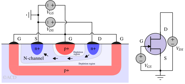
In Figure 6, a more realistic diagram of JFET operation is shown. The depletion width is wider near the drain region, choking the channel. The depletion region is narrow near the source region, so the channel is wider. Since the channel is wider near the source region, the control of the channel current lies on the Gate-Source voltage once the drain region is pinched off.
Current-voltage relationship of a JFET
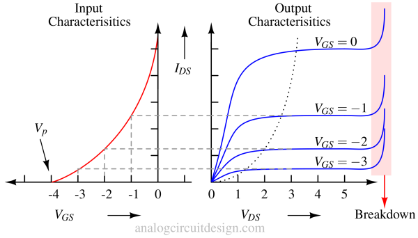
- Input characteristics (IDS vs. VGS): As VGS decreases (with a high magnitude in the negative direction), the IDS decreases as the depletion region chokes the channel. The IDS vs. VGS curve is quadratic, as shown in Figure 8. The IDS is maximum when VGS\=0. The current becomes zero when a large reverse bias is applied.
- Output characteristics (IDS vs. VDS): With lower VDS voltage, the current is approximately proportional to VDS. After some VDS, the IDS becomes constant. The voltage after which the drain current becomes constant is called VDS(sat). This flat region of current is called the pinched region. In this region, the drain voltage does not affect the channel current (IDS). The transistor can be used as a voltage-controlled current source in this region.
JFET regions of operation
A JFET's output characteristics (IDS vs. VDS) can be categorized into the following regions of operation:
- Ohmic region (VDS < VGS - Vp)
- Pinch-off (VDS > VGS - Vp)
- Cut-off (VGS < Vp)
- Breakdown region (VDS > VDSS)
Ohmic region
Here in this region, the depletion region is not wide enough to pinch-off the channel region.
$$I_{DS} = I_{DSS}\left[2\left(1-\cfrac{V_{GS}}{V_p}\right)\left(\cfrac{V_{DS}}{-V_p}\right)-\left(\cfrac{V_{DS}}{V_p}\right)^2\right]$$
For small VDS (drain-source voltage), the JFET's drain-source terminal acts as a resistor. VGS sets the resistance across the drain and source.
Pinch-off
In (current)saturation region, the channel pinch-off is achieved by VDS. If VDS > VGS-Vp, the channel is pinched-off from charge carriers near the drain and VDS loses control over IDS. So, the IDS saturates to a value decided by VGS only.
$$I_{DS} = I_{DSS}\left(1-\cfrac{V_{GS}}{V_p}\right)^2$$
There is still some weak control left of VDS to IDS. That is due to channel length modulation. Due to this, the IDS increases with VDS. It can be captured by using the following equation :
$$I_{DS} = I_{DSS}\left(1-\cfrac{V_{GS}}{V_p}\right)^2\left(1+\lambda{}V_{DS}\right)$$
Cut-off
In the cut-off region, VGS achieves channel pinch-off. If VGS < Vp, the channel is entirely devoid of charge carriers, and IDS becomes zero.
$$I_{DS} = 0$$
Breakdown region
Due to the high electric field in the depletion region due to high VGS, avalanche multiplication happens. Due to this, the current increases rapidly with VDS, as shown in Figure 8. If the current is not controlled through a series resistor, the device may heat up quickly and get destroyed.
A rise in gate current can be observed during avalanche breakdown. The gate current changes direction when the avalanche breakdown happens.
Difference between of MOSFET and JFET
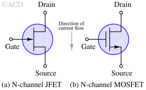
A MOSFET has an oxide insulator between the gate and the channel. So, in the symbol, there is a gap between the gate and the channel.
In a JFET, there is no oxide insulator. There is a PN junction when forward bias can push current into the channel through the gate. Therefore, the gate is directly connected to the channel in JFET.
JFET has a lower input impedance (~108Ω) than a MOSFET. However, it offers a much higher input impedance than a BJT. MOSFET has a much higher input impedance (~1010-1015Ω) due to its insulating gate.
JFETs are more robust and less prone to damage as their junctions are more durable and can handle higher voltage and currents. On the other hand, MOSFET gates are extremely sensitive because the gate insulator is extremely thin (a few nanometres) and can be easily damaged by even a tiny overvoltage.
JFET operates only in depletion mode, while a MOSFET can operate in enhancement and depletion modes.
JFET parameters
Transconductance (gm)
Transconductance indicates how effectively the JFET can control the drain current with the gate-source voltage. It is defined mathematically as the ratio of change in drain current with change in gate-source voltage:
$$g_m=\cfrac{\Delta{}I_D}{\Delta{}V_{GS}}$$
$$g_m=-\cfrac{2I_{DSS}}{V_p}\left(1-\cfrac{V_{GS}}{V_p}\right)$$
A higher gm means the JFET is more responsive to changes in VGS, which is beneficial for amplification applications. The unit of transconductance is Siemens (S) or A/V (amperes per volt). The transconductance (gm) varies with the operating po\int of the JFET, particularly with VGS.
Input impedance (Zin)
The input impedance of a Junction Field Effect Transistor (JFET) is notably high, typically 108 Ω or more in the low-frequency regions. This is true for common-source and common-drain configurations. This characteristic is primarily due to the reverse-biased nature of the gate junction, which prevents significant current flow into the gate terminal.
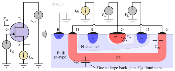
$$Z_{in}=R_{in}||\cfrac{1}{j\omega{}C_{in}}$$
$$C_{in}=C_{gb}+C_{gd}$$
The input impedance also has a capacitive component due to the gate capacitance (typically in the picofarad range). At high frequencies, impedance decreases due to the reactance of the gate capacitance. The dominant factor in the input impedance is the gate (specifically the back gate) to bulk capacitance.
Output impedance (Zout)
JFETs generally exhibit a high output impedance, typically in the range of 103 and 106 ohms. This characteristic is beneficial for minimizing loading effects on the preceding stages in a circuit, allowing for better amplification (gain).
JFET amplifiers
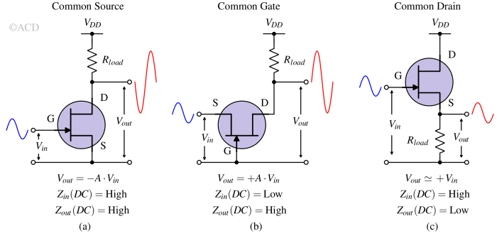
- Common-Source (CS) amplifier: In the common-source amplifier, as shown in Fig 11(a), the input is applied to the gate, and the output is taken from the drain. It offers high voltage gain and high input impedance. The output is inverted (180° phase shift). The input impedance is higher than BJT's common-emitter configuration but lower than MOSFET's common-source configuration. Used as voltage amplification stage.
- Common Gate (CG) Amplifier: The input is applied to the source as shown in Fig 11(b), and the output is taken from the drain. It offers low input impedance and high output impedance. There is no phase inversion at the output. It is used for high-frequency amplification because it provides a higher bandwidth than the common-source amplifier.
- Common Drain (CD) Amplifier (Source Follower): The input is applied to the gate as shown in Fig 11(c), and the output is taken from the source. It offers high input impedance, low output impedance, and unity voltage gain (no phase inversion). Used for impedance matching and buffering.